MAX5426 查看數據表(PDF) - Maxim Integrated
零件编号
产品描述 (功能)
生产厂家
MAX5426 Datasheet PDF : 9 Pages
| |||
Precision Resistor Network for
Programmable Instrumentation Amplifiers
ABSOLUTE MAXIMUM RATINGS
VDD to GND ............................................................-0.3V to +17V
VSS to GND.............................................................-17V to +0.3V
D0, D1 to GND ...........................................-0.3V to (VDD + 0.2V)
D0, D1 to GND (VDD > +6V) .................................-0.3V to +6.0V
All Other Pins to GND ......................(VSS - 0.3V) to (VDD + 0.2V)
Maximum Current Into VDD, VSS, D1, D0 .........................±50mA
Maximum Current from OUT1 to CM or OUT2 ..............±0.72mA
Maximum Current from OUT1 to INDIF- or OUT............±0.72mA
Maximum Current from OUT2 to INDIF+ or OFFSET.....±0.72mA
Continuous Power Dissipation (TA = +70°C)
14-Pin TSSOP (derate 9.1mW/°C above +70°C) ..........727mW
Operating Temperature Range ...........................-40°C to +85°C
Junction Temperature ......................................................+150°C
Storage Temperature Range .............................-60°C to +150°C
Stresses beyond those listed under “Absolute Maximum Ratings” may cause permanent damage to the device. These are stress ratings only, and functional
operation of the device at these or any other conditions beyond those indicated in the operational sections of the specifications is not implied. Exposure to
absolute maximum rating conditions for extended periods may affect device reliability.
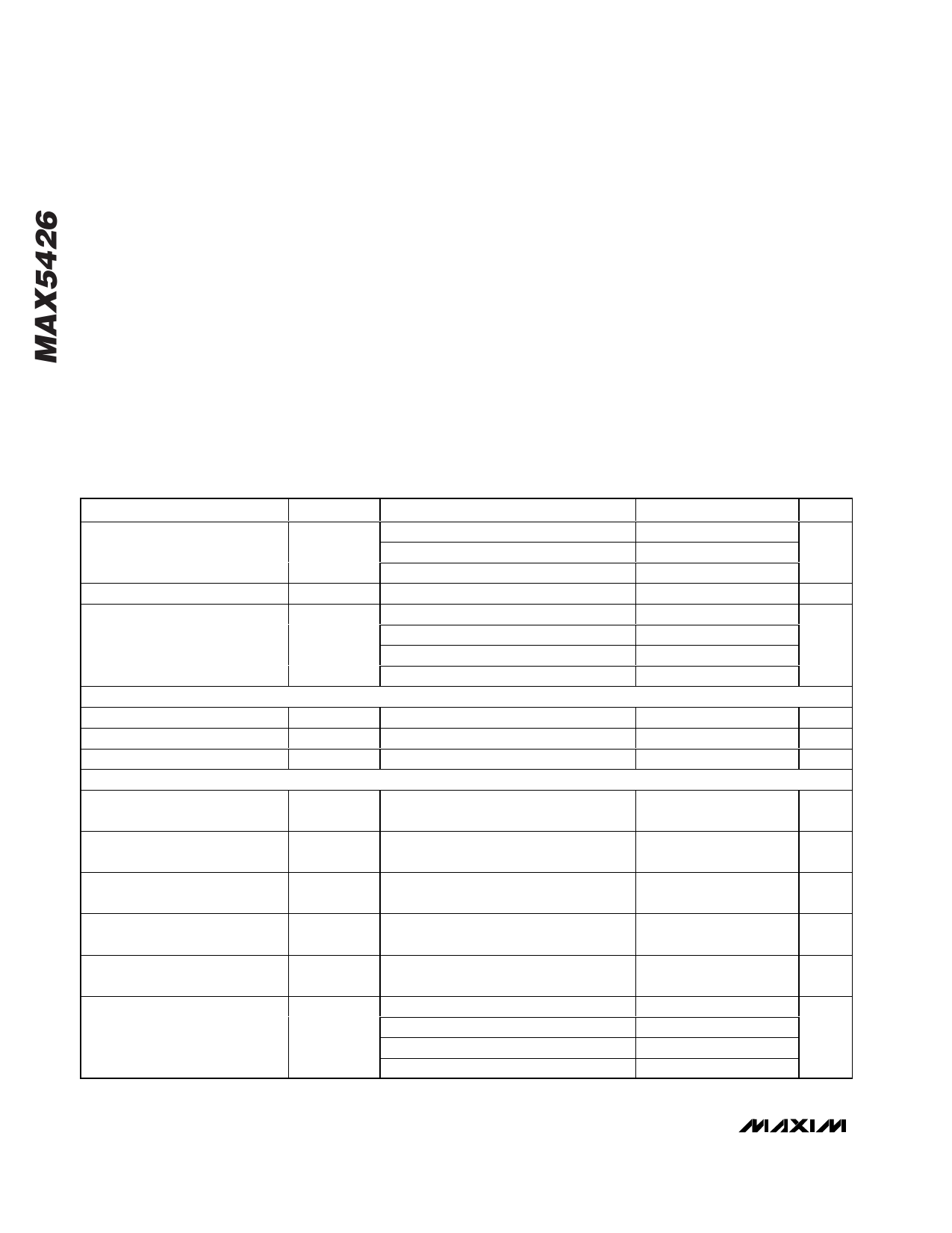
ELECTRICAL CHARACTERISTICS
(VDD = +15V, VSS = -15V, GND = 0, TA = TMIN to TMAX, unless otherwise noted. Typical values are at TA = +25°C.)
PARAMETER
SYMBOL
CONDITIONS
MAX5426A
Gain Range Accuracy (Notes 1, 2)
MAX5426B
MAX5426C
Capacitance at Analog Pins
CANALOG
Gain = 1
Differential CMRR (Notes 1, 2)
Gain = 2
Gain = 4
Gain = 8
DIGITAL INPUTS
Input High Voltage
Input Low Voltage
Input Leakage Current
EQUIVALENT RESISTANCES
VIH
VIL
ILKG
D1 = D0 = 0 or logic high
Resistance Between OUT1 and
OUT2
ROUT1, ROUT2
MIN TYP MAX
0.004 0.025
0.025 0.090
0.080 0.500
5
79
85
91
97
2.4
0.8
10
56
Resistance Between OUT1 and
INDIF-
ROUT1, RINDIF-
26
Resistance Between INDIF- and
OUT
RINDIF-, ROUT
26
Resistance Between OUT2 and
INDIF+
ROUT2, RINDIF+
26
Resistance Between INDIF+ and
OFFSET
RINDIF+,
ROFFSET
26
Gain = 1
0
Resistance Between OUT1 and
FB1
Gain = 2
ROUT1, RFB1 Gain = 4
15
22
Gain = 8
26
UNITS
%
pF
dB
V
V
µA
kΩ
kΩ
kΩ
kΩ
kΩ
kΩ
2 _______________________________________________________________________________________
Share Link: 