K9G4G08B0A 查看數據表(PDF) - Samsung
零件编号
产品描述 (功能)
生产厂家
K9G4G08B0A Datasheet PDF : 44 Pages
| |||
K9L8G08U1A
K9G4G08U0A K9G4G08B0A
Preliminary
FLASH MEMORY
Product Introduction
The K9G4G08X0A is a 4,224Mbit(4,429,185,024bit) memory organized as 262,144 rows(pages) by 2,112x8 columns. Spare 64 col-
umns are located from column address of 2,048~2,111. A 2,112-byte data register is connected to memory cell arrays for accommo-
dating data transfer between the I/O buffers and memory cells during page read and page program operations. The memory array is
made up of 32 cells that are serially connected to form a NAND structure. Each of the 32 cells resides in a different page. A block
consists of two NAND structured strings. A NAND structure consists of 32 cells. A cell has 2-bit data. Total 1,081,344 NAND cells
reside in a block. The program and read operations are executed on a page basis, while the erase operation is executed on a block
basis. The memory array consists of 2,048 separately erasable 256K-byte blocks. It indicates that the bit by bit erase operation is pro-
hibited on the K9G4G08X0A.
The K9G4G08X0A has addresses multiplexed into 8 I/Os. This scheme dramatically reduces pin counts and allows system upgrades
to future densities by maintaining consistency in system board design. Command, address and data are all written through I/O's by
bringing WE to low while CE is low. Those are latched on the rising edge of WE. Command Latch Enable(CLE) and Address Latch
Enable(ALE) are used to multiplex command and address respectively, via the I/O pins. Some commands require one bus cycle. For
example, Reset Command, Status Read Command, etc require just one cycle bus. Some other commands, like page read and block
erase and page program, require two cycles: one cycle for setup and the other cycle for execution. The 528M-byte physical space
requires 30 addresses, thereby requiring five cycles for addressing : 2 cycles of column address, 3 cycles of row address, in that
order. Page Read and Page Program need the same five address cycles following the required command input. In Block Erase oper-
ation, however, only three row address cycles are used. Device operations are selected by writing specific commands into the com-
mand register. Table 1 defines the specific commands of the K9G4G08X0A.
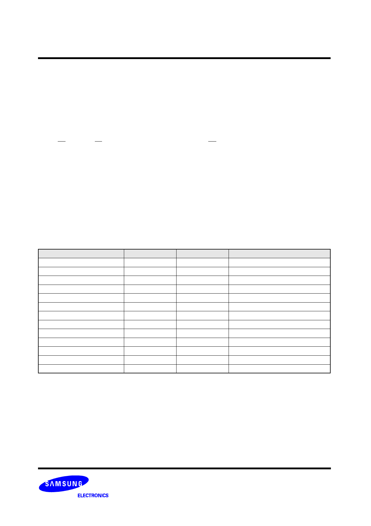
Table 1. Command Sets
Function
Read
Two-Plane Read
Read ID
Reset
Page Program
Two-Plane Page Program (2)
Block Erase
Two-Plane Block Erase
Random Data Input(1)
Random Data Output(1)
Two Plane Random Data Output(3)
Read Status 1
Read Status 2
1st Cycle
00h
60h----60h
90h
FFh
80h
80h----11h
60h
60h----60h
85h
05h
00h----05h
70h
F1h
2nd Cycle
30h
30h
-
-
10h
81h----10h
D0h
D0h
-
E0h
E0h
-
-
Acceptable Command during Busy
O
O
O
NOTE : 1. Random Data Input/Output can be executed in a page.
2. Any command between 11h and 81h is prohibited except 70h/F1h and FFh.
3. Two-Plane Random Data Output msut be used after Two-Plane Read operation.
Caution : Any undefined command inputs are prohibited except for above command set of Table 1.
9
Share Link: 