MAX1717 查看數據表(PDF) - Maxim Integrated
零件编号
产品描述 (功能)
生产厂家
MAX1717 Datasheet PDF : 33 Pages
| |||
Dynamically Adjustable, Synchronous
Step-Down Controller for Notebook CPUs
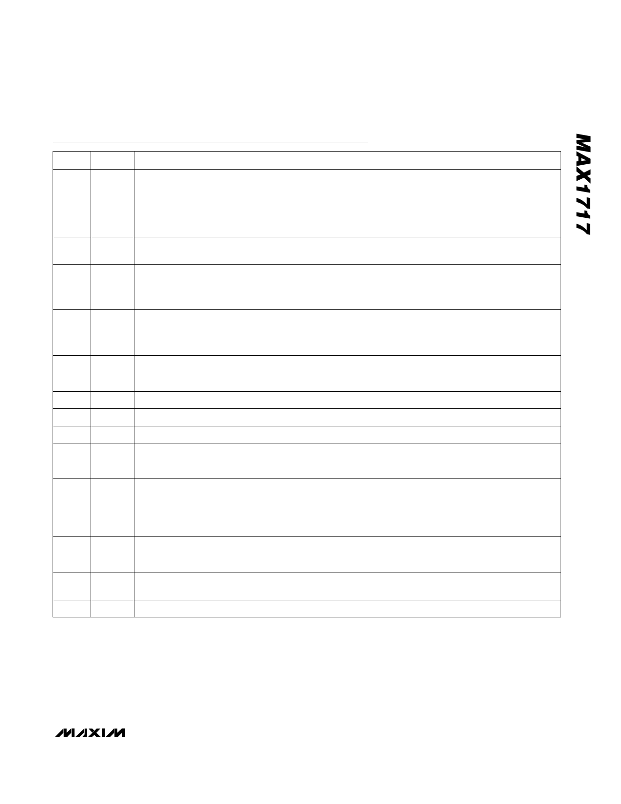
Pin Description (continued)
PIN
8
9
10
11
12
13
14
15
16
17–21
22
23
24
NAME
TON
REF
ILIM
GNDS
VGATE
GND
DL
VDD
A/B
D4–D0
BST
LX
DH
FUNCTION
On-Time Selection Control Input. This is a four-level input that sets the K factor (Table 3) to determine
DH on-time. Connect TON to the following pins for the indicated operation:
GND = 1000kHz
REF = 550kHz
Open = 300kHz
VCC = 200kHz
2V Reference Output. Bypass to GND with 0.22µF (min) capacitor. Can source 50µA for external loads.
Loading REF degrades FB accuracy according to the REF load-regulation error.
Current-Limit Adjustment. The GND - LX current-limit threshold defaults to 100mV if ILIM is tied to VCC. In
adjustable mode, the current-limit threshold voltage is 1/10th the voltage seen at ILIM over a 0.5V to 3.0V
range. The logic threshold for switchover to the 100mV default value is approximately VCC - 1V. Tie ILIM to
REF for a fixed 200mV threshold.
Ground Remote-Sense Input. For nonvoltage-positioned circuits, connect GNDS to ground directly at the
load. GNDS internally connects to the integrator that fine tunes the output voltage. The output voltage rises
by an amount of GNDS - GND. For voltage-positioned circuits, increase the output voltage (24mV (typ)) by
biasing GNDS with a resistor-divider from REF to GND.
Open-Drain Power-Good Output. VGATE is normally high when the output is in regulation. VGATE goes low
whenever the DAC code changes, and returns high one clock period after the slew-rate controller finishes
and the output is in regulation. VGATE is low in shutdown.
Analog and Power Ground. Also connects to the current-limit comparator.
Low-Side Gate Driver Output. DL swings GND to VDD.
Supply Voltage Input for the DL Gate Driver, 4.5V to 5.5V. Bypass to GND with a 1µF capacitor.
Internal MUX Select Input. When A/B is high, the DAC code is determined by logic-level voltages on D0–D4.
On the falling edge of A/B (or during power-up with A/B low), the DAC code is determined by the resistor
values at D0–D4.
DAC Code Inputs. D0 is the LSB and D4 is the MSB for the internal 5-bit DAC (see Table 4). When A/B is
high, D0–D4 function as high-input-impedance logic inputs. On the falling edge of A/B (or during power-up
with A/B low), the series resistance on each input sets its logic state as follows:
(series resistance ≤ 1kΩ ±5%) = logic low
(series resistance ≥ 100kΩ ±5%) = logic high
Boost Flying Capacitor Connection. Connect BST to the external boost diode and capacitor as shown in the
Standard Application Circuit. An optional resistor in series with BST allows the DH pullup current to be
adjusted (Figure 5).
Inductor Connection. LX is the internal lower supply rail for the DH high-side gate driver. It also connects to
the current-limit comparator and the skip-mode zero-crossing comparator.
High-Side Gate-Driver Output. DH swings LX to BST.
______________________________________________________________________________________ 11
Share Link: 