AD8225 查看數據表(PDF) - Analog Devices
零件编号
产品描述 (功能)
生产厂家
AD8225 Datasheet PDF : 16 Pages
| |||
AD8225
+VS
+VS
+VS
VB
–IN
Q2
Q1
+IN
–VS R2
A1
C2
A2
C1
R1 –VS +VS
3k⍀
A3
15k⍀
3k⍀
15k⍀
+VS
–VS
VREF
OUT
–VS
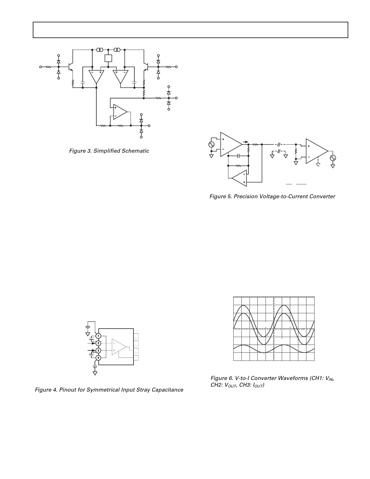
Figure 3. Simplified Schematic
THEORY OF OPERATION
The AD8225 is a monolithic, three op amp instrumentation
amplifier. Laser wafer trimming and proprietary circuit tech-
niques enable the AD8225 to boast the lowest output offset
voltage and drift of any currently available in amp (150 µV
RTI), as well as a higher common-mode voltage range.
Referring to Figure 3, the input buffers consist of super-beta
NPN transistors Q1 and Q2, and op amps A1 and A2. The
transistors are compensated so that the bias currents are
extremely low, typically 100 pA or less. As a result, current noise
is also low, at 50 fA/√Hz. The unity gain input buffers drive a
gain-of-five difference amplifier. Because the 3 kΩ and 15 kΩ
resistors are ratio matched, gain stability is better than 5 ppm/°C
over the rated temperature range.
The AD8225 also has five times the gain bandwidth of a typical
in amp. This wider GBW results from compensation at a fixed
gain of 5, which can be one fifth of that required if the amplifier
were compensated for unity gain.
High frequency performance is also enhanced by the innovative
pinout of the AD8225. Since Pins 1 and 8 are uncommitted,
Pin 1 may be connected to Pin 4. Since Pin 4 is also ac com-
mon, the stray capacitance at Pins 2 and 3 is balanced.
AC
GROUND
–IN
+IN
AC
GROUND
AD8225
8 NC
7 +VS
6 VOUT
5 REF
PIN 1 HAS NO INTERNAL CONNECTION
Figure 4. Pinout for Symmetrical Input Stray Capacitance
APPLICATIONS
Precision V-to-I Converter
When small analog voltages are transmitted across significant
distances, errors may develop due to ambient electrical noise,
stray capacitance, or series impedance effects. If the desired
voltage is converted to a current, however, the effects of ambient
noise are mitigated. All that is required is a voltage to current
conversion at the source, and an I-to-V conversion at the other
end to reverse the process.
Figure 5 illustrates how the AD8225 may be used as the trans-
mitter and receiver in a current loop system. The full-scale
output is 5 mA.
eIN
200mV
pk FS
3
IOUT
RSH
20⍀
AD8225 6
2
5
1k⍀
VSH
47pF
9k⍀
OP27
FULL SCALE
CURRENT = 5mA
8⍀
3
AD8225 6
2
5
GND OR
REF V
IOUT
=
VSH
RSH
=
0.5 eIN
RSH
eOUT
200mV
pk FS
Figure 5. Precision Voltage-to-Current Converter
As noted in Figure 5, an additional op amp and four resistors are
required to complete the converter. The precision gain of 5 in the
AD8225s, used in the transmit and receive sections, preserves
the integrity of the desired signal, while the high frequency
common-mode performance at the receiver rejects noise on the
transmission line. The reference of the receiver may be connected
to local ground or the reference pin of an A/D converter (ADC).
Figure 6 shows bench measurements of the input and output
voltages, and output current of the circuit of Figure 5. The
transmission media is 10 feet of insulated hook-up wire for the
current drive and return lines.
eIN = 398mV p-p, eOUT = 398mV p-p,
IOUT = 10.3mA p-p
1
eIN
eOUT
2
IOUT
3
CH 1 = 100mV, CH 2 = 100mV, CH 3 = 10mA,
H = 200s
Figure 6. V-to-I Converter Waveforms (CH1: VIN,
CH2: VOUT, CH3: IOUT)
REV. A
–11–
Share Link: 