AD9286(Rev0) 查看數據表(PDF) - Analog Devices
零件编号
产品描述 (功能)
生产厂家
AD9286 Datasheet PDF : 28 Pages
| |||
AD9286
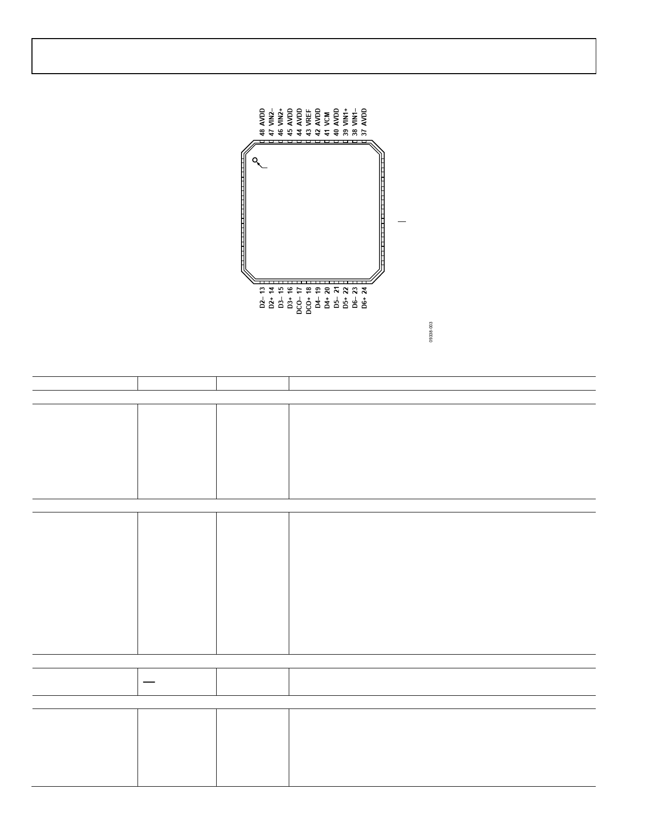
PIN CONFIGURATION AND FUNCTION DESCRIPTIONS
AVDD 1
AVDD 2
AUXCLK+ 3
AUXCLK– 4
RBIAS 5
AUXCLKEN 6
DRGND 7
DRVDD 8
D0– (LSB) 9
D0+ (LSB) 10
D1– 11
D1+ 12
PIN 1
INDICATOR
AD9286
TOP VIEW
(Not to Scale)
36 AVDD
35 AVDD
34 CLK+
33 CLK–
32 CSB
31 SDIO/PWDN
30 SCLK
29 OE
28 DRGND
27 DRVDD
26 D7+ (MSB)
25 D7– (MSB)
NOTES
1. THE EXPOSED PADDLE MUST BE SOLDERED TO THE PCB ANALOG
GROUND TO ENSURE PROPER FUNCTIONALITY AND HEAT
DISSIPATION, NOISE, AND MECHANICAL STRENGTH BENEFITS.
Figure 6. Pin Configuration
Table 8. Pin Function Descriptions
Pin No.
Mnemonic
ADC Power Pins
1, 2, 35, 36, 37, 40, 42,
44, 45, 48
AVDD
8, 27
DRVDD
7, 28
DRGND
0
AGND
ADC Analog Pins
39
38
46
47
43
5
41
34
33
3
4
Digital Inputs
6
29
Digital Outputs
26
25
24
23
VIN1+
VIN1−
VIN2+
VIN2−
VREF
RBIAS
VCM
CLK+
CLK−
AUXCLK+
AUXCLK−
AUXCLKEN
OE
D7+ (MSB)
D7− (MSB)
D6+
D6−
Type
Description
Supply
Supply
Ground
Ground
Analog Power Supply (1.8 V Nominal).
Digital Output Driver Supply (1.8 V Nominal).
Digital Output Ground.
Analog Ground. Pin 0 is the exposed thermal pad on the bottom of the
package. This is the only ground connection, and it must be soldered to
the PCB analog ground to ensure proper functionality and heat dissipation,
noise, and mechanical strength benefits.
Input
Input
Input
Input
Input/output
Input/output
Output
Input
Input
Input
Input
Differential Analog Input Pin (+) for Channel 1.
Differential Analog Input Pin (−) for Channel 1.
Differential Analog Input Pin (+) for Channel 2.
Differential Analog Input Pin (−) for Channel 2.
Voltage Reference Input/Output.
External Reference Bias Resistor. Connect 10 kΩ from RBIAS to AGND.
Common-Mode Level Bias Output for Analog Inputs.
ADC Clock Input—True.
ADC Clock Input—Complement.
Auxiliary ADC Clock Input—True.
Auxiliary ADC Clock Input—Complement.
Input
Input
Auxiliary Clock Input Enable.
Digital Enable (Active Low) to Tristate Output Data Pins.
Output
Output
Output
Output
Output Data 7—True.
Output Data 7—Complement.
Output Data 6—True.
Output Data 6—Complement.
Rev. 0 | Page 10 of 28
Share Link: 