ADJD-S313-QR999 查看數據表(PDF) - Avago Technologies
零件编号
产品描述 (功能)
生产厂家
ADJD-S313-QR999 Datasheet PDF : 16 Pages
| |||
Data format
ADJD-S313 uses a register-based programming
architecture. Each register has a unique address and
controls a specific function inside the chip.
To write to a register, the master first generates a
START condition. Then it sends the slave address
for the device it wants to communicate with. The
least significant bit (LSB) of the slave address must
indicate that the master wants to write to the slave.
The addressed device will then acknowledge the
master.
The master writes the register address it wants to
access and waits for the slave to acknowledge. The
master then writes the new register data. Once the
slave acknowledges, the master generates a STOP
condition to end the data transfer.
To read from a register, the master first generates
a START condition. Then it sends the slave address
for the device it wants to communicate with. The
least significant bit (LSB) of the slave address must
indicate that the master wants to write to the slave.
The addressed device will then acknowledge the
master.
The master writes the register address it wants to
access and waits for the slave to acknowledge. The
master then generates a repeated START condition
and resends the slave address sent previously. The
least significant bit (LSB) of the slave address must
indicate that the master wants to read from the
slave. The addressed device will then acknowledge
the master.
The master reads the register data sent by the slave
and sends a no acknowledge signal to stop reading.
The master then generates a STOP condition to end
the data transfer.
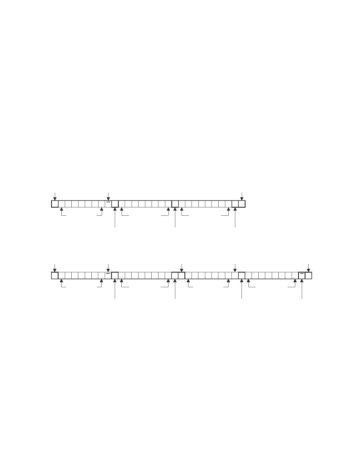
Start condition
Master will write data
Stop condition
S A6 A5 A4 A3 A2 A1 A0 W A D7 D6 D5 D4 D3 D2 D1 D0 A D7 D6 D5 D4 D3 D2 D1 D0 A P
Master sends
slave address
Master writes
register address
Master writes
register data
Slave acknowledge
Slave acknowledge
Slave acknowledge
Figure 8. Register Byte Write Protocol
Start condition
Master will write data
Repeated start
condition
Master will read data
Stop condition
S A6 A5 A4 A3 A2 A1 A0 W A D7 D6 D5 D4 D3 D2 D1 D0 A Sr A6 A5 A4 A3 A2 A1 A0 R A D7 D6 D5 D4 D3 D2 D1 D0 A P
Master sends
slave address
Master writes
register address
Master sends
slave address
Master reads
register data
Slave acknowledge
Slave acknowledge
Slave acknowledge
Master not
acknowledge
Figure 9. Register Byte Read Protocol
11
Share Link: 