AMMC-6231-W10 查看數據表(PDF) - Avago Technologies
零件编号
产品描述 (功能)
生产厂家
AMMC-6231-W10 Datasheet PDF : 8 Pages
| |||
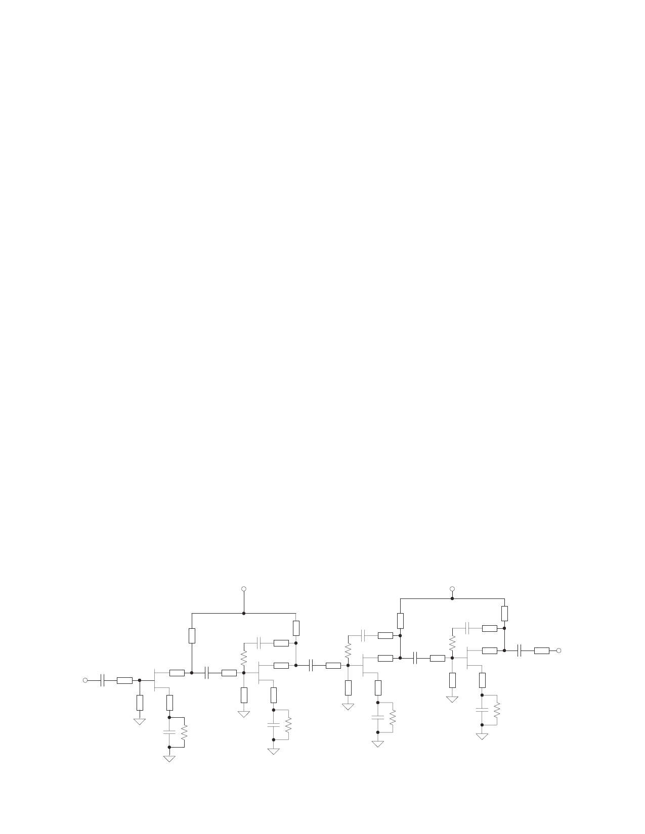
Biasing and Operation
The AMMC-6231 is normally biased with a positive
supply connected to both VD1 and VD2 bond pads
through the 100pF bypass capacitor as shown in
Figure 21. The recommended supply voltage is 3
V. It is important to place the bypass capacitor as
close to the die as possible. No negative gate bias
voltage is needed for the AMMC-6231. Input and
output matching are achieved on-die, therefore no
other external component is required besides one
100pF bypass capacitor for the main supply. The
input and output are DC-blocked with internal
coupling capacitors.
No ground wires are needed because all ground
connections are made with plated through-holes
to the backside of the device.
Refer the Absolute Maximum Ratings table for
allowed DC and thermal conditions.
Assembly Techniques
The backside of the MMIC chip is RF ground. For
microstrip applications the chip should be attached
directly to the ground plane (e.g. circuit carrier or
heatsink) using electrically conductive epoxy [1]
For best performance, the topside of the MMIC
should be brought up to the same height as the
circuit surrounding it. This can be accomplished
by mounting a gold plate metal shim (same length
and width as the MMIC) under the chip which is
of correct thickness to make the chip and adjacent
circuit the same height. The amount of epoxy
used for the chip and/or shim attachment should
be just enough to provide a thin fillet around the
bottom perimeter of the chip or shim. The ground
plan should be free of any residue that may
jeopardize electrical or mechanical attachment.
The location of the RF bond pads is shown in
Figure 12. Note that all the RF input and output
ports are in a Ground-Signal-Ground configuration.
RF connections should be kept as short as
reasonable to minimize performance degradation
due to undesirable series inductance. A single
bond wire is normally sufficient for signal
connections, however double bonding with 0.7 mil
gold wire or use of gold mesh [2] is recommended
for best performance, especially near the high end
of the frequency band.
Thermosonic wedge bonding is preferred method
for wire attachment to the bond pads. Gold mesh
can be attached using a 2 mil round tracking tool
and a tool force of approximately 22 grams and a
ultrasonic power of roughly 55 dB for a duration
of 76 +/- 8 mS. The guided wedge at an untrasonic
power level of 64 dB can be used for 0.7 mil
wire. The recommended wire bond stage
temperature is 150 +/- 2C.
Caution should be taken to not exceed the Absolute
Maximum Rating for assembly temperature and
time.
The chip is 100um thick and should be handled
with care. This MMIC has exposed air bridges on
the top surface and should be handled by the
edges or with a custom collet (do not pick up the
die with a vacuum on die center).
This MMIC is also static sensitive and ESD
precautions should be taken
Notes:
[1] Ablebond 84-1 LM1 silver epoxy is recommended.
[2] Buckbee-Mears Corporation, St. Paul, MN, 800-262-3824
VD1
VD2
RFout
RFin
Figure 17. AMMC-6231 Simplified Schematic
7
Share Link: 