AN8022L 查看數據表(PDF) - Panasonic Corporation
零件编号
产品描述 (功能)
生产厂家
AN8022L Datasheet PDF : 16 Pages
| |||
Voltage Regulators
s Application Notes (continued)
[2] Operation descriptions (continued)
4. Overcurrent protection circuit (OVP) (continued)
0
CLM (−)
Terminal
voltage
VTH (−200 mV typ.)
AN8022L, AN8022SB
Overshoot
due to
delay
Time
Pulse width can not be made
shorter than this width due to delay
VOUT
Terminal
voltage
0
Time
Power
MOSFET
current
0
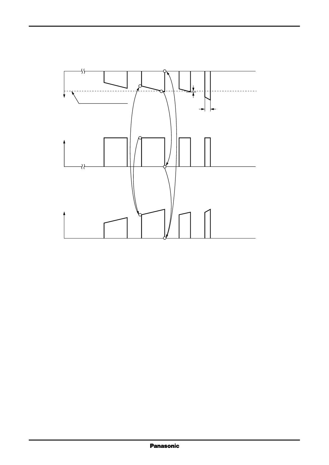
Figure 6. Pulse-by-pulse overcurrent detector operation waveform
Time
5. Soft start
At start of the power supply, the capacitor connected to the power supply output causes the power supply to
rise under overload condition. Under this condition, the power supply output is low. For the normal PWM control,
attempt is made to limit the current by the pulse-by-pulse over current protection so that the power supply output
could rise at maximum duty. However, pulses can not be made down to zero due to circuit delay. As a result, large
current flows in the mains switch (the power MOSFET) or in the diode in the secondary side, and in the worst case
these parts are damaged.
For this reason, soft start function in which the power supply output does not rise with maximum duty but rise
with gradually widening duty from the minimum one (0%) at the power supply start is adopted.
The use of this function requires more rise time of power supply output. However, it can extend the service
life of parts and raise the reliability of the power supply.
The soft start (SS) terminal is connected to the PWM input (hereinafter its voltage is referred to as VSS). In the
PWM, three voltages are input: the voltage to which the current feedback level is converted (hereinafter referred
to as VFB), the voltage determining the maximum duty (hereinafter referred to as VDTC). This voltage is determined
inside the IC), and the triangular wave oscillation voltage (hereinafter referred to as VCT). VSS , VFB and VDTC are
input in the non-reverse input (+) of the PWM comparator and VCT is input in the reverse input (−). Among the three
signals of the non-reverse input, the lowest one is selected for input to the PWM comparator.
The external capacitor (hereinafter referred to as CSS) is connected to the SS terminal. In the pre-start condition,
this capacitor is set to be sufficiently discharged by the transistor inside the IC.
When the supply voltage exceeds the start voltage to start the IC operation, charging is started in the CSS by
the constant current source inside the IC. Therefore VSS gradually rises from 0 V.
11
Share Link: 