APT7846 查看數據表(PDF) - Anpec Electronics
零件编号
产品描述 (功能)
生产厂家
APT7846 Datasheet PDF : 15 Pages
| |||
APT7846
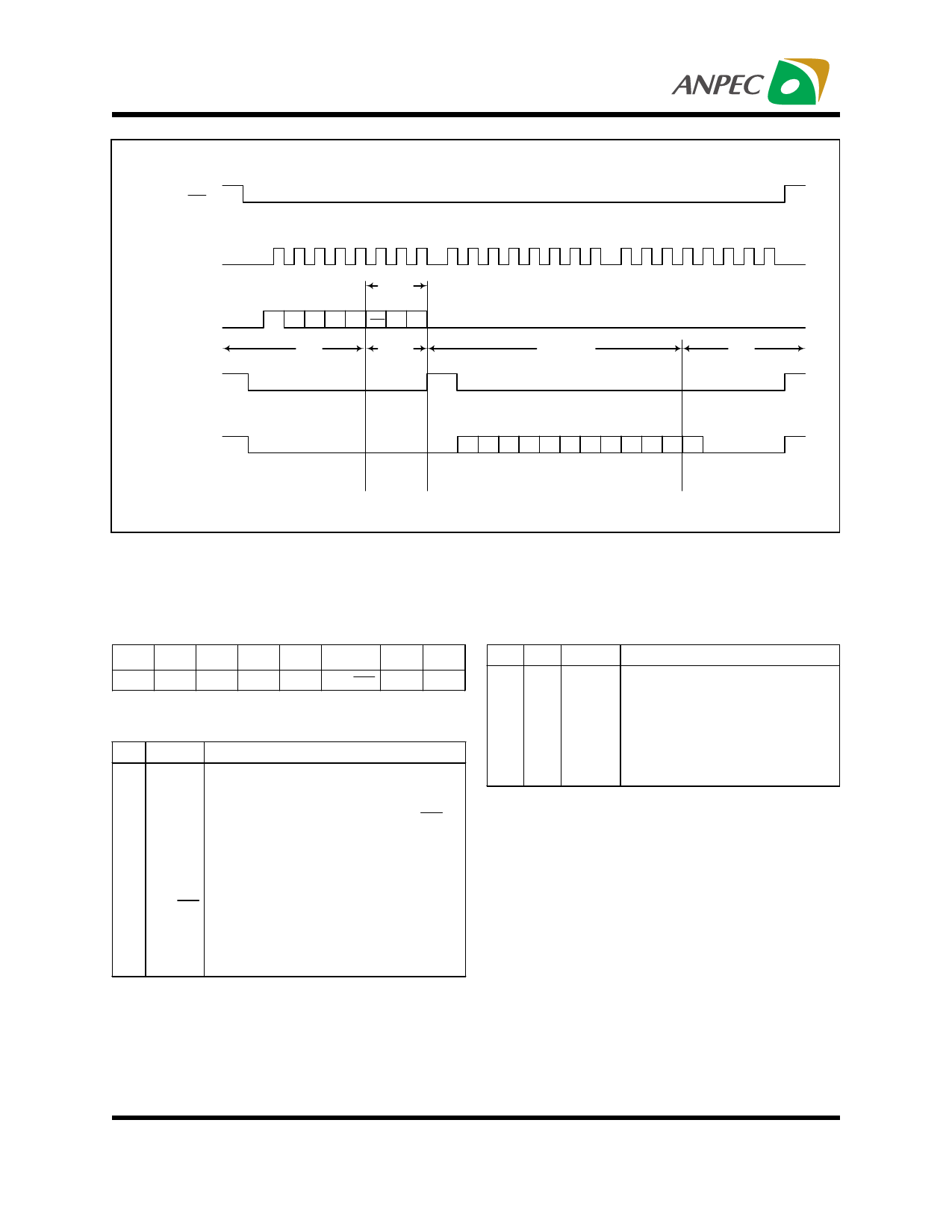
CS
DCLK
DIN
BUSY
1
81
tACQ
S A2 A1
(START)
ldle
A0
MODE
SER/
DFR
2,
2,
Acquire
81
Conversion
8
ldle
DOUT
11 10 9 8 7 6 5 4 3 2 1 0
(MSB)
(LSB)
FIGURE 5. Conversion Timing , 24-Clocks per Conversion , 8-bit Bus Interface. No DCLK Delay Required
with Dedicated Serial Port.
Bit 7 Bit 6 Bit 5 Bit 4 Bit 3
(MSB)
Bit 2
Bit 1 Bit 0
(LSB)
S
A2
A1
A0 MODE SER/DFR PD1 PD0
TABLE III. Order of the Control Bits in the Control
Byte.
BIT NAME DESCRIPTION
7
S
Start Bit. Control byte starts with first HIGH bit on
DIN. A new control byte can start every 15th clock
cycle in 12-bit conversion mode or every 11th clock
cycle in 8-bit conversion mode.
6-4 A2-A0 Channel Select Bits. Along with the SER/DFR bit,
these bits control the setting of the multiplexer
input, switches, and reference inputs, as detailed in
Tables I and II.
3 MODE 12-Bit/8-Bit Conversion Select Bit. This bit controls
the number of bits for the following conversion: 12-
bits(LOW) or 8-bits(HIGH).
2 SER/DFR Single-Ended/Differential Reference Select Bit.
Along with bits A2-A0, this bit controls the setting of
the multiplexer input, switches, and reference
inputs, as detailed in Tables I and II.
1-0 PD1-PD0 Power-Down Mode Select Bits. See Table V for
details.
TABLE IV. Descriptions of the Control Bits within the
Control Byte.
PD1 PD0 PENIRQ DESCRIPTION
Power-down between conversions. When
0
0 Enabled each conversion is finished, the converter
enters a low power mode.
0
1 Enabled Reference is OFF.
1
0 Enabled Reference is ON
1
1
Disabled
No power-down between
device is always powered.
conversions,
TABLE V. Power-Down Selection.
Copyright ANPEC Electronics Corp.
8
Rev. A.6 - Dec., 2001
www.anpec.com.tw
Share Link: 