AV3168 查看數據表(PDF) - Unspecified
零件编号
产品描述 (功能)
生产厂家
AV3168 Datasheet PDF : 24 Pages
| |||
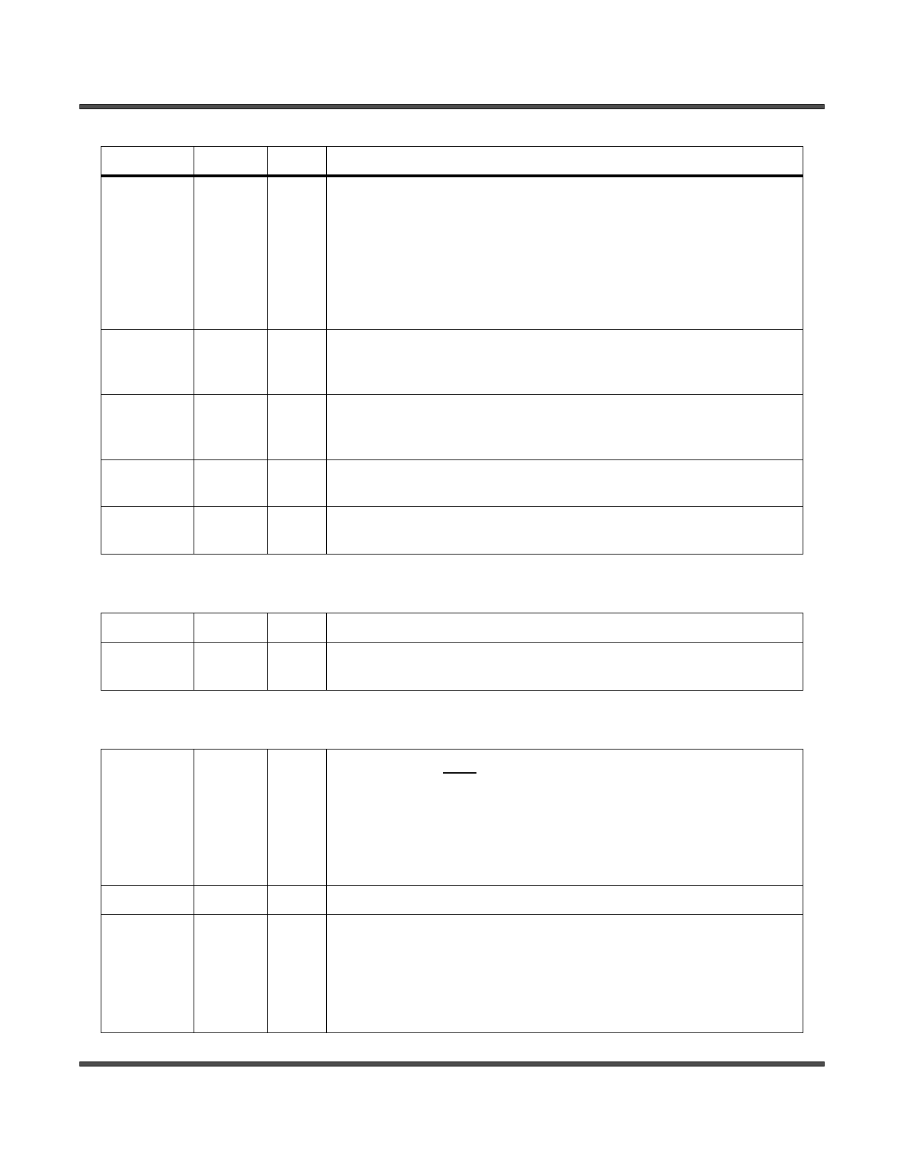
AV3168/69
PIN DESCRIPTIONS (Continued)
Pin Name
C
Pin #
33
Type
Description
O Analog video output
Determined by the state of CPNT pin and CR0[5:4]
CPNT CR0[5] CR0 [4]
--- 0 ------ X------X: --S-Video C output.
---- 1 ------ X-----0:---Cb output in YCbCr component mode
--1 1 ------ 0 ---- X:1111111- ::
--1 1 ------ 1------1:--Green color output in RGB mode
VREF
IREF
COMP
BIAS
40
I/O Voltage reference. It has an internal voltage reference circuit, but may
be overridden by an external voltage reference input. A 0.1 uF ceramic
capacitor is required between this pin and GND.
39
I A resistor should be connected between this pin and GND to control the
DAC output current. The recommended value is 198 (382) ohm 1%
metal film resistor for double (single) end 75 ohm termination.
38
I Compensation capacitor for the DAC internal reference amplifier. A 0.1
uF ceramic capacitor is required between this pin and VDDA.
37
I/O DAC bias voltage. A 0.1 uf ceramic capacitor must be used to de-
couple this pin to VDDA.
SERIALCONTRL BUS
SCL
24
I Serial bus clock
SDA
23
I/0 Serial bus address and data input and output pin.
Open drain output.
CLOCK SIGNALS
GCK
7
CK27
9
ACK
25
O General Purpose Clock. Clock frequency is determined by the state of
GOUT[1:0] when RST pin is low.
00 : 40.5 MHz clock output.
0 1: 54.0 MHz clock output.
1 0: 67.5 Mhz clock output.
1 1: 81.0 MHz
O 27 MHz clock output pin.
I/O 384*fs Audio clock output pin.
Controlled by CR2[1:0]
0 0: 384 * 48.0 KHz (18.432MHz) clock output.
0 1: 384 * 44.1 KHz (16.934MHz) clock output.
1 0. 384 * 96.0 KHz (36.864MHz) clock output.
1 1: 384 * 88.2 KHz (33.868MHz) clock output.
7-24
January 4, 2001
Share Link: 