XRD9815 查看數據表(PDF) - Exar Corporation
零件编号
产品描述 (功能)
生产厂家
XRD9815 Datasheet PDF : 44 Pages
| |||
XRD9815
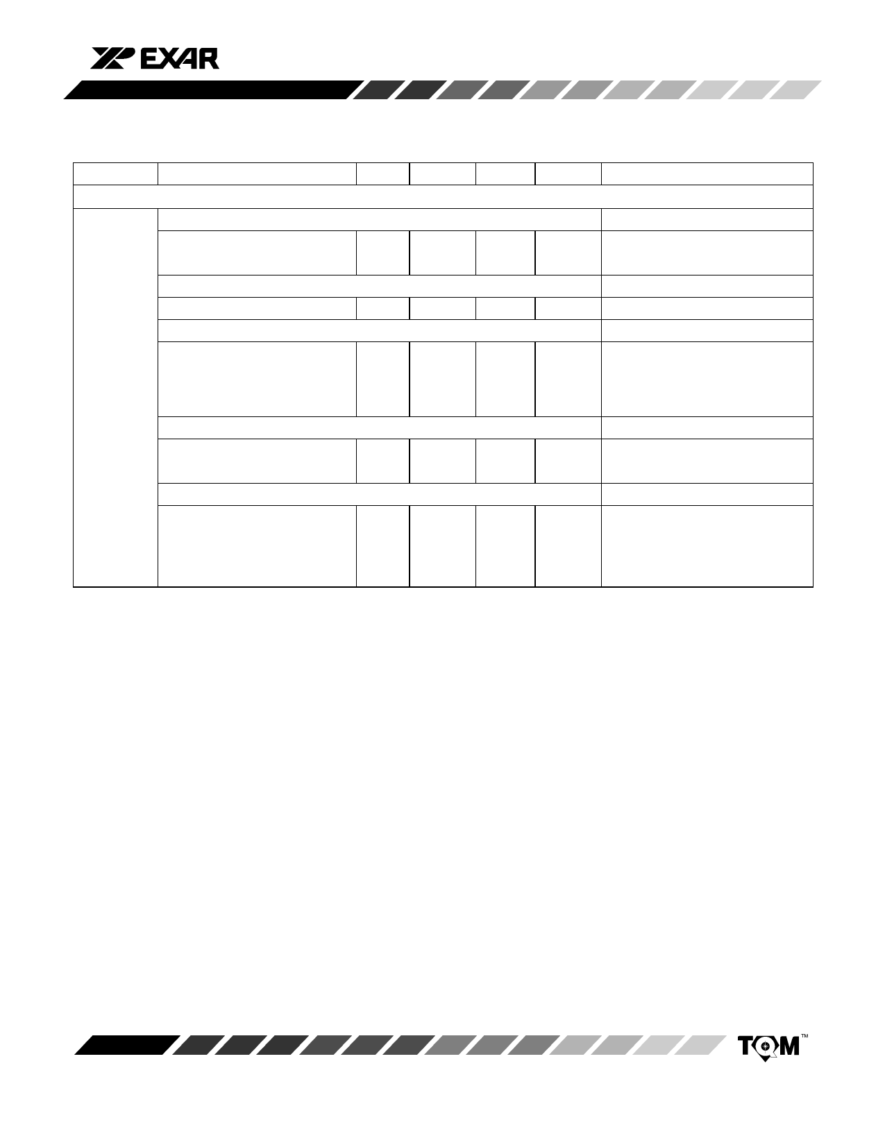
ELECTRICAL CHARACTERISTICS (CONT’D)
Test Conditions: AVDD=DVDD=5.0V, ADCCLK=12MHz, TA=25°C unless otherwise specified.
Symbol Parameter
Min.
Typ.
Max.
Unit Conditions
SYSTEM SPECIFICATIONS (Includes CDS, PGA and A/D)
Differential Non-Linearity
DNLSMIN
PGA Gain= 00h (min)
+/-0.5
LSB
DNLSMAX
PGA Gain= ffh (max)
+/-0.5
LSB
Integral Non--Linearity (3-Channel CDS Mode)
INLSMIN
PGA Gain= 00h (min)
Input Referred Noise
+/-3.0
LSB
IRNSMIN
PGA Gain = 00h (min)
1
mV rms 3V, A/D FSR, Conf. Reg. #1,
PB5=1
IRNSMAX
PGA Gain = ffh (max)
250
mV rms 3V, A/D FSR, Conf. Reg. #1,
PB5=1
Output Referred Offset
OROSMIN
PGA Gain= 00h (min)
+/-50
mV
OROSMAX
PGA Gain = ffh (max)
+/-150
mV
Input Referred Offset Adjustment Range (Note 1 & 2)
IROSMIN
IROSMID
IROSMAX
PGA Gain = 00h (min)
PGA Gain = 80h
PGA Gain = ffh (max)
-135
-12.5
0
110
mV
9.3
mV
0
mV Guaranteed to Remove Internal
Offsets Only
Notes:
1 The “Input Referred Offset Adjustment Range is guaranteed for both CDS and S/H modes.
2 Please see Graph 1-4 on page 16 for typical “Input Referred Offset Adjustment Range.”
Rev. 5.10
7
Share Link: 