CMX881 查看數據表(PDF) - CML Microsystems Plc
零件编号
产品描述 (功能)
生产厂家
CMX881 Datasheet PDF : 59 Pages
| |||
PMR Signalling Processor
CMX881
signal (e.g. RSSI) these components are not required. The values of C9 and R10 set the attack
time, C9 and R9 set the decay time. D1 can be any suitable small signal diode. R10 should be a
high enough value so as not to distort the signal source.
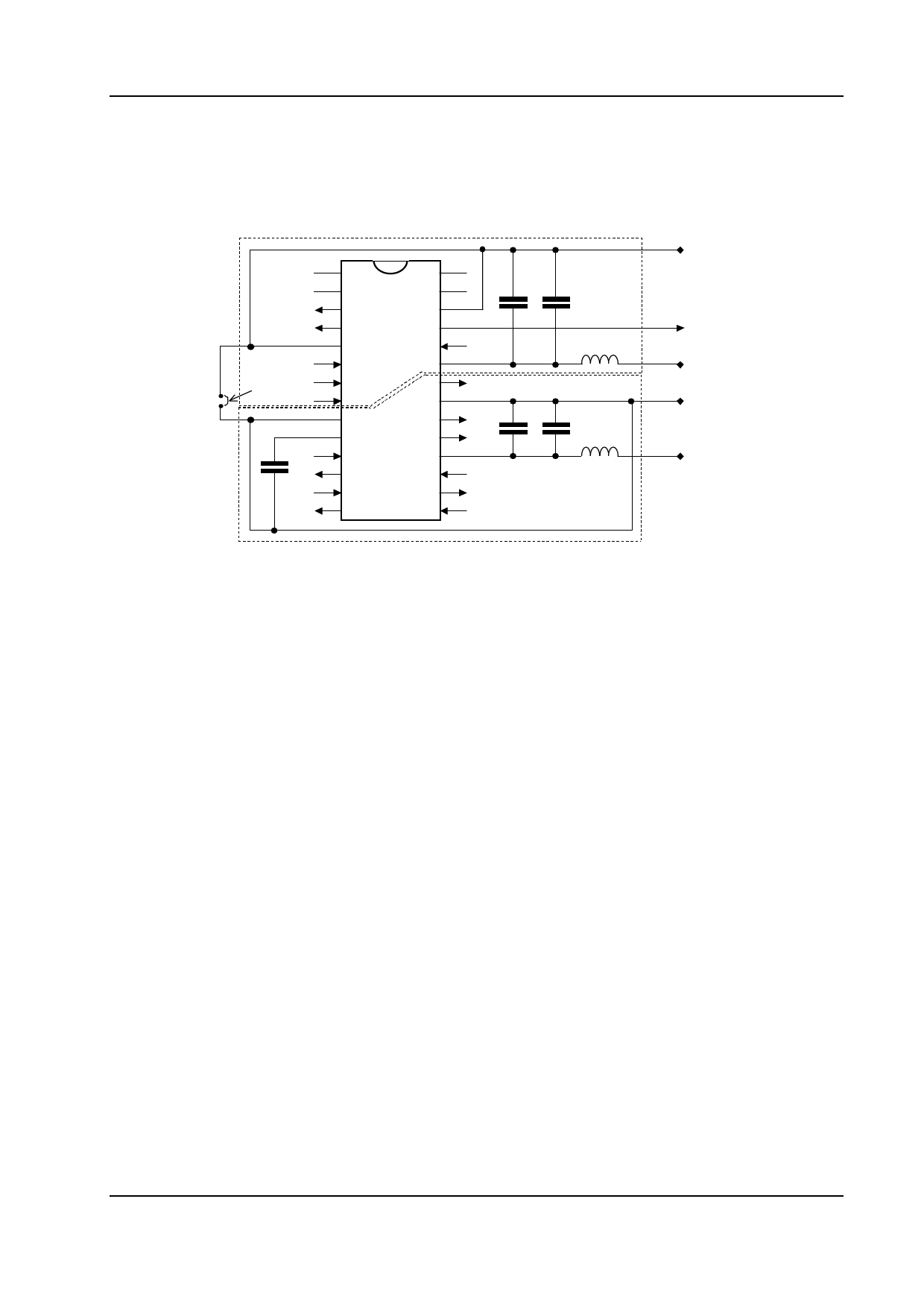
1.4.1 PCB Layout Guidelines and Power Supply Decoupling
VSS(D)
provision for
wire link
VSS(A)
VBIAS
C15
1
28
2
27
3
26
4
25
5
24
6 CM X881 23
7
22
8
21
9
20
10
19
11
18
12
17
13
16
14
15
C11
VDD(D)
VSS(A)
C13
VDD(A)
Digital Ground
Digit al
ground plane
C12
+
Clock Output
L1
Digital +ve Supply
Analogue Ground
C14
+
L2
Analogue +ve Supply
Analogue
ground plane
Figure 3 Power Supply Connections and De-coupling
C11 10nF
C12 10µF
C13 10nF
C14 10µF
C15 100nF
L1 100nH
L2 100nH
See note 7
See note 7
Resistors ±5%, capacitors and inductors ±20% unless otherwise stated.
Notes:
7. The inductors L1 and L2 can be omitted but this may degrade system performance.
It is important to protect the analogue pins from extraneous inband noise and to minimise the impedance
between the CMX881 and the supply and bias de-coupling capacitors. The de-coupling capacitors C11,
C12, C13 and C14 should be as close as possible to the CMX881, particularly C11 and C13. It is
therefore recommended that the printed circuit board is laid out with separate ground planes for the
VSS(A) and VSS(D) in the area of the CMX881, with provision to make a link between them close to the
CMX881.
VBIAS is used as an internal reference for detecting and generating the various analogue signals. It must
be carefully decoupled, to ensure its integrity, so apart from the decoupling capacitor shown, no other
loads should be connected. If VBIAS needs to be used to set the discriminator mid-point reference, it
must be buffered with a high input impedance buffer.
The single ended microphone input(s) and audio output must be ac coupled as shown, so their return
paths can be connected to VSS(A) without introducing dc offsets. Further buffering of the audio output is
advised.
The crystal X1 can be replaced with an external clock source if required/desired. The internal clock
generating circuit can be placed in power-save mode if the clock is provided externally.
2004 CML Microsystems Plc
11
D/881/7
Share Link: 