DS1845 查看數據表(PDF) - Dallas Semiconductor -> Maxim Integrated
零件编号
产品描述 (功能)
生产厂家
DS1845 Datasheet PDF : 13 Pages
| |||
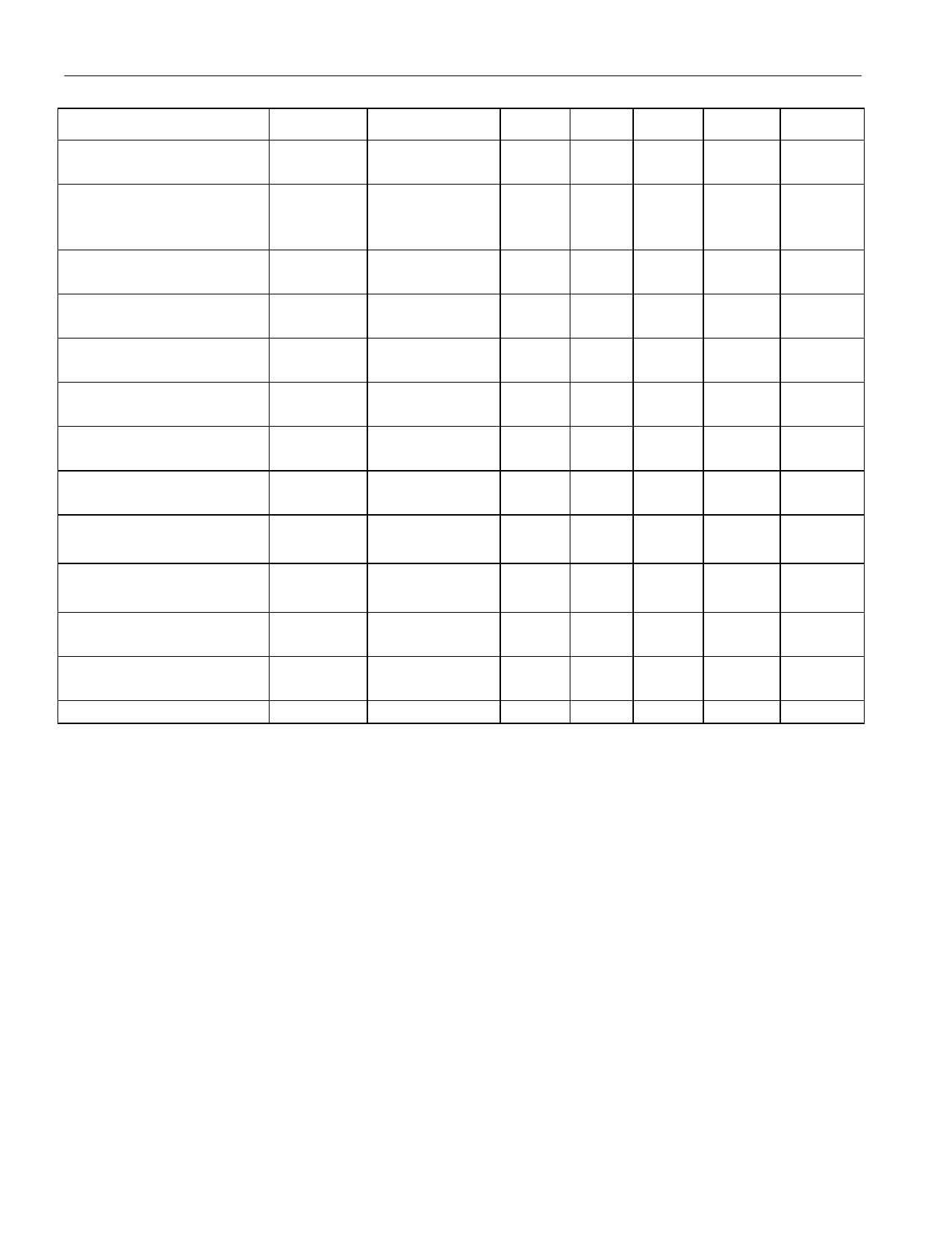
AC ELECTRICAL CHARACTERISTICS
PARAMETER
SYMBOL CONDITION
SCL clock frequency
fSCL
Bus free time between
STOP and START
condition
Hold time (repeated)
START condition
Low period of SCL clock
tBUF
tHD:STA
tLOW
High period of SCL clock tHIGH
Data hold time
tHD:DAT
Data set-up time
tSU:DAT
Start set-up time
tSU:STA
Rise time of both SDA
and SCL signals
Fall time of both SDA
and SCL signals
Set-up time for STOP
condition
Capacitive load for each
bus line
EEPROM write time
* fast mode
** standard mode
tR
tF
tSU:STO
CB
TW
DS1845
(-40oC to 85oC, Vcc=2.7V to 5.5V)
MIN TYP MAX UNITS NOTES
0
400 kHz
*,6
0
100
**
1.3
µs
*,6
4.7
**
0.6
4.0
1.3
4.7
0.6
4.0
0
0
100
250
0.6
4.7
20+0.1
CB
20+0.1
CB
0.6
4.0
µs
µs
µs
0.9
µs
ns
µs
300
ns
1000
300
ns
300
µs
400
pF
*,7,6
**
*,6
**
*,6
**
*,6,8
**
*,6
**
*,6
**
*,9
**
*,9
**
*
**
9
5
ms
10
NOTES:
1. All voltages are referenced to ground.
2. ISTBY specified with for VCC equal 3.0V and 5.0V and control port logic pins are driven to the
appropriate logic levels. Appropriate logic levels specify that logic inputs are within a 0.5V of
ground or VCC for the corresponding inactive state.
3. I/O pins of fast mode devices must not obstruct the SDA and SCL lines if VCC is switched off.
4. Address Inputs, A0, A1, and A2, should be tied to either VCC or GND depending on the desired
address selections.
5. ISTBY specified with for VCC equal 3.0V and 5.0V and control port logic pins are driven to the
appropriate logic levels. Appropriate logic levels specify that logic inputs are within a 0.5V of
ground or VCC for the corresponding inactive state.
11 of 13
Share Link: 