HDD16M72D9W 查看數據表(PDF) - Hanbit Electronics Co.,Ltd
零件编号
产品描述 (功能)
生产厂家
HDD16M72D9W
Hanbit Electronics Co.,Ltd

HDD16M72D9W Datasheet PDF : 11 Pages
| |||
HANBit
HDD16M72D9W
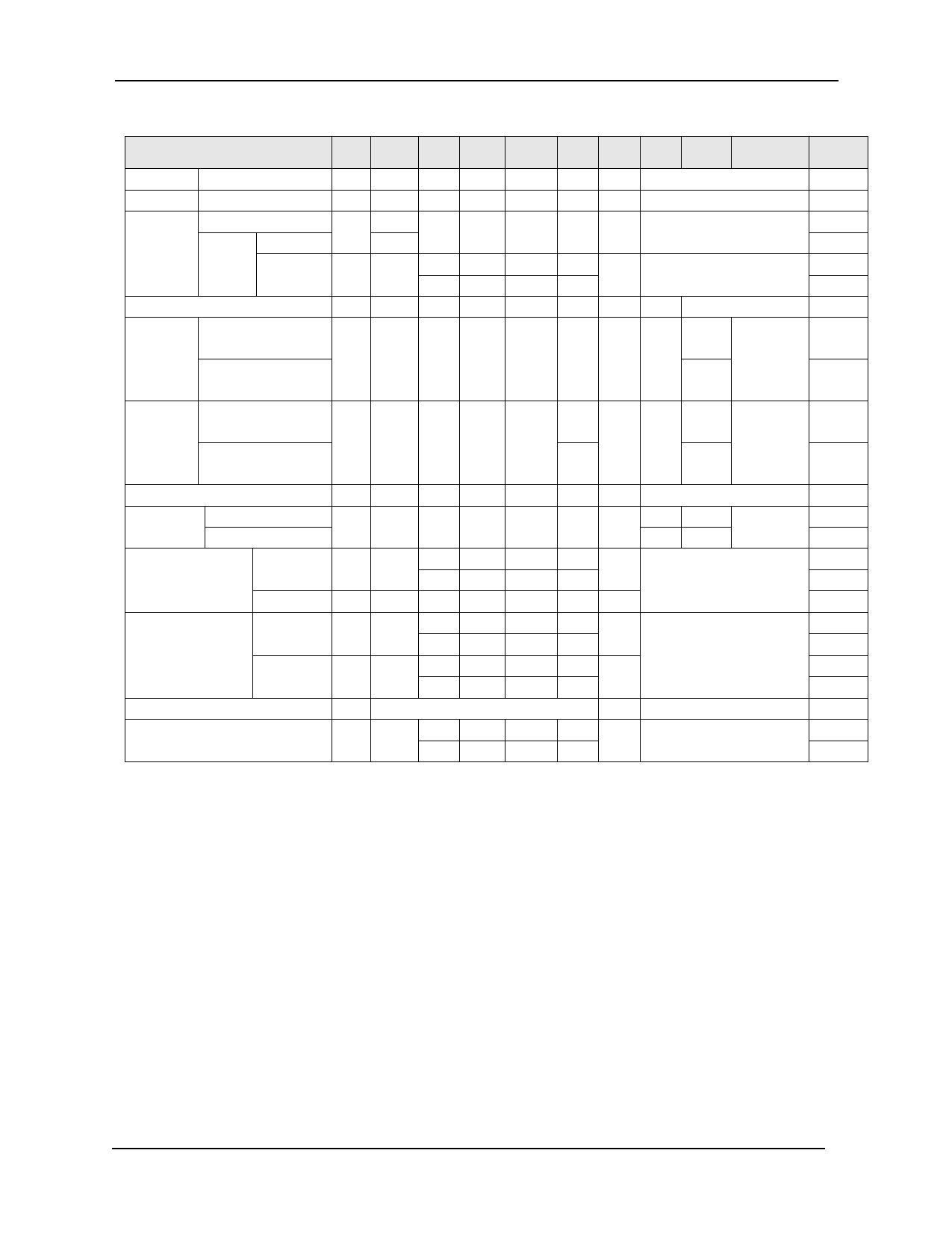
COMMAND TRUTH TABLE (V=Valid, X=Don’t Care, H=Logic High, L=Logic Low)
COMMAND
CK
E
n-1
CKE
n
/CS /RAS /CAS /WE DM
BA
0,1
Register
Extended MRS
HX
L
L
L
LX
Register Mode register set H
X
L
L
L
LX
Auto refresh
H
H
L
L
L
HX
Entry
L
Refresh Self
L
H
H
H
refresh
Exit
L
H
X
H
X
X
X
Bank active & Row Addr.
H
X
L
L
H
HXV
Auto precharge
Read &
disable
column
H
X
L
H
L
HXV
Auto precharge
address
eable
Auto precharge
Write &
H
disable
column
H
X
L
H
L
XV
Auto precharge
address
L
enable
Burst Stop
H
X
L
H
H
LX
Bank selection
V
Precharge
H
X
L
L
H
LX
All banks
X
H
X
X
X
Clock suspend or
Entry
H
L
X
L
V
V
V
active power down
Exit
L
H
X
X
X
XX
H
X
X
X
Entry
H
L
X
Precharge power
L
H
H
H
down mode
H
X
X
X
Exit
L
H
X
L
V
V
V
DM
H
X
V
No operation command
H
X
X
X
HX
X
L
H
H
H
Note :
1. OP Code : Operand Code. A0 ~ A12 & BA0 ~ BA1 : Program keys. (@EMRS/MRS)
A10/
AP
A11
A9~A0
OP code
OP code
X
X
Row address
L
Column
Address
H (A0 ~ A9)
L
Column
Address
H (A0 ~ A9)
X
L
X
H
X
X
X
X
NOTE
1,2
1,2
3
3
3
3
4
4
4
4,6
7
5
8
2. EMRS/ MRS can be issued only at all banks precharge state.
A new command can be issued 2 clock cycles after EMRS or MRS.
3. Auto refresh functions are same as the CBR refresh of DRAM.
The automatical precharge without row precharge command is meant by "Auto".
Auto/self refresh can be issued only at all banks precharge state.
4. BA0 ~ BA1 : Bank select addresses.
If both BA0 and BA1 are "Low" at read, write, row active and precharge, bank A is selected.
If BA0 is "High" and BA1 is "Low" at read, write, row active and precharge, bank B is selected.
If BA0 is "Low" and BA1 is "High" at read, write, row active and precharge, bank C is selected.
If both BA0 and BA1 are "High" at read, write, row active and precharge, bank D is select ed.
5. If A10/AP is "High" at row precharge, BA0 and BA1 are ignored and all banks are selected.
6. During burst write with auto precharge, new read/write command can not be issued.
Another bank read/write command can be issued after the end of burst.
New row active of the associated bank can be issued at tRP after the end of burst.
7. Burst stop command is valid at every burst length.
8. DM sampled at the rising and falling edges of the DQS and Data -in are masked at the both edges (Write DM latency is 0).
9. This combination is not defined for any function, which means "No Operation(NOP)" in DDR SDRAM.
URL : www.hbe.co.kr
REV 1.0 (November.2002)
9
HANBit Electronics Co.,Ltd.
Share Link: