HI-1573 查看數據表(PDF) - Holt Integrated Circuits
零件编号
产品描述 (功能)
生产厂家
HI-1573 Datasheet PDF : 11 Pages
| |||
HI-1573, HI-1574
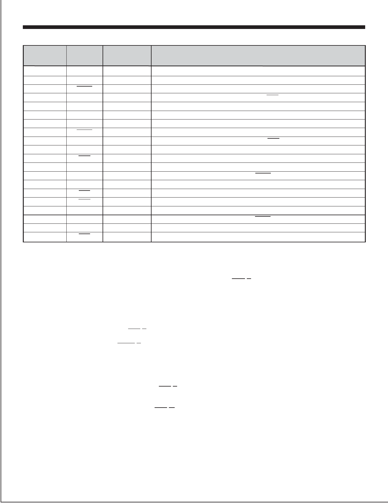
PIN DESCRIPTIONS
PIN
(DIP & SOIC) SYMBOL FUNCTION
1
VDDA
power supply
2
BUSA
analog
3
BUSA
analog
4
RXENA
digital input
5
GNDA
power supply
6
VDDB
power supply
7
BUSB
analog
8
BUSB
analog
9
RXENB
digital input
10
GNDB
power supply
11
RXB
digital output
12
RXB
digital output
13
TXINHB
digital input
14
TXB
digital input
15
TXB
digital input
16
RXA
digital output
17
RXA
digital output
18
TXINHA
digital input
19
TXA
digital input
20
TXA
digital input
DESCRIPTION
+3.3 volt power for transceiver A
MIL-STD-1533 bus driver A, positive signal
MIL-STD-1553 bus driver A, negative signal
Receiver A enable. If low, forces RXA and RXA low (HI-1573) or High (HI-1574)
Ground for transceiver A
+3.3 volt power for transceiver B
MIL-STD-1533 bus driver B, positive signal
MIL-STD-1553 bus driver B, negative signal
Receiver B enable. If low, forces RXB and RXB low (HI-1573) or High (HI-1574)
Ground for transceiver B
Receiver B output, inverted
Receiver B output, non-inverted
Transmit inhibit, bus B. If high BUSB, BUSB disabled
Transmitter B digital data input, non-inverted
Transmitter B digital data input, inverted
Receiver A output, inverted
Receiver A output, non-inverted
Transmit inhibit, bus A. If high BUSA, BUSA disabled
Transmitter A digital data input, non-inverted
Transmitter A digital data input, inverted
FUNCTIONAL DESCRIPTION
The HI-1573 family of data bus transceivers contains differ-
ential voltage source drivers and differential receivers. They
are intended for applications using a MIL-STD-1553 A/B
data bus. The device produces a trapezoidal output wave-
form during transmission.
The receiver’s differential input stage drives a filter and
threshold comparator that produces CMOS data at the
RXA/B and RXA/B output pins. When the MIL-STD-1553
bus is idle and RXENA or RXENB are high, RXA/B will be
logic “0” on HI-1573 and logic “1” on HI-1574.
TRANSMITTER
The receiver outputs are forced to the bus idle state (logic "0”
on HI-1573 or logic “1” on HI-1574) when RXENA or RXENB
Data input to the device’s transmitter section is from the com- is low.
plementary CMOS inputs TXA/B and TXA/B. The transmit-
ter accepts Manchester II bi-phase data and converts it to dif- MIL-STD-1553 BUS INTERFACE
ferential voltages on BUSA/B and BUSA/B. The transceiver
outputs are either direct- or transformer-coupled to the MIL- A direct-coupled interface (see Figure 2) uses a 1:2.5 ratio
STD-1553 data bus. Both coupling methods produce a nomi- isolation transformer and two 55 ohm isolation resistors
nal voltage on the bus of 7.5 volts peak to peak.
between the transformer and the bus. The primary center-
tap of the isolation transformer must be connected to GND.
The transmitter is automatically inhibited and placed in the
high impedance state when both TXA/B and TXA/B are In a transformer-coupled interface (see Figure 2), the
driven with the same logic state. A logic “1” applied to the transceiver is connected to a 1:1.79 isolation transformer
TXINHA/B input will force the transmitter to the high imped- which in turn is connected to a 1:1.4 coupling transformer.
ance state, regardless of the state of TXA/B and TXA/B.
The transformer-coupled method also requires two coupling
resistors equal to 75% of the bus characteristic impedence
RECEIVER
(Zo) between the coupling transformer and the bus.
The receiver accepts bi-phase differential data from the MIL-
STD-1553 bus through the same direct- or transformer-
coupled interface as the transmitter.
Figure 3 and Figure 4 show test circuits for measuring
electrical characteristics of both direct- and transformer-
coupled interfaces respectively. (See electrical
characteristics on the following pages).
HOLT INTEGRATED CIRCUITS
2
Share Link: 