HSD4M64D4B 查看數據表(PDF) - Hanbit Electronics Co.,Ltd
零件编号
产品描述 (功能)
生产厂家
HSD4M64D4B
Hanbit Electronics Co.,Ltd

HSD4M64D4B Datasheet PDF : 10 Pages
| |||
HANBit
HSD4M64D4B
Notes :
1. VIH (max) = 5.6V AC. The overshoot voltage duration is ≤ 3ns.
2. VIL (min) = -2.0V AC. The undershoot voltage duration is ≤ 3ns.
3. Any input 0V ≤ VIN ≤ VDDQ.
Input leakage currents include Hi-Z output leakage for all bi-directional buffers with Tri-State outputs.
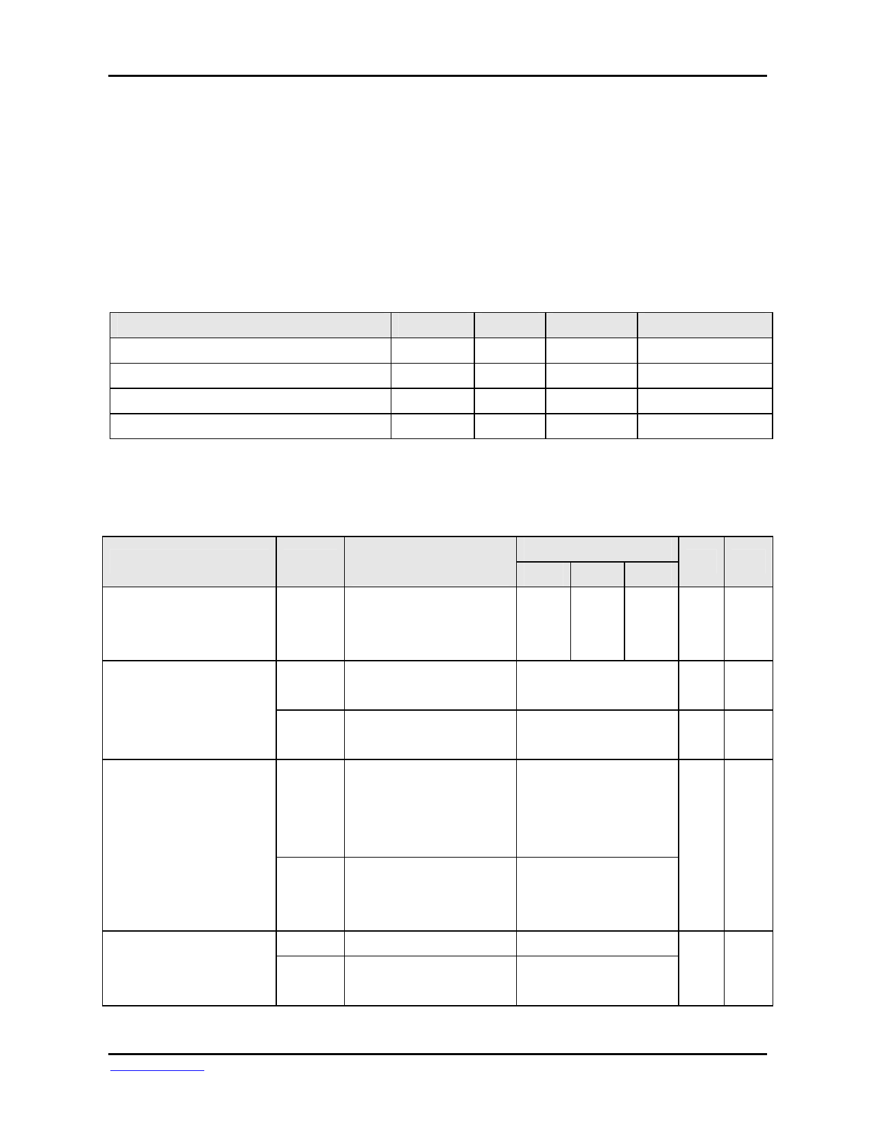
CAPACITANCE
(VCC = 3.3V, TA = 23°C, f = 1MHz, VREF =1.4V ± 200 mV)
DESCRIPTION
SYMBOL
MIN
Clock
/RAS, /CAS,/WE,/CS, CKE, L(U)DQM
Address
DQ (DQ0 ~ DQ15)
CCLK
15
CIN
30
CADD
30
COUT
5
MAX
25
40
40
15
UNITS
pF
pF
pF
pF
DC CHARACTERISTICS
(Recommended operating condition unless otherwise noted, TA = 0 to 70°C)
PARAMETER
SYMBOL
TEST
CONDITION
VERSION
80
10
10L
Operating current
(One bank active)
Burst length = 1
ICC1
tRC ≥ tRC(min)
IO = 0mA
300
280
280
CKE ≤ VIL(max)
ICC2P
4
Precharge standby current in
tCC=10ns
power-down mode
CKE & CLK ≤ VIL(max)
ICC2PS
4
tCC=∞
CKE ≥ VIH(min)
CS* ≥ VIH(min), tCC=10ns
ICC2N
48
Input signals are changed
Precharge standby current in
one time during 20ns
non power-down mode
CKE ≥ VIH(min)
ICC2NS
CLK ≤ VIL(max), tCC=∞
24
Input signals are stable
ICC3P
CKE ≤ VIL(max), tCC=10ns
8
Active standby current in
CKE&CLK ≤ VIL(max)
power-down mode
ICC3PS
8
tCC=∞
UNIT NOTE
mA
1
mA
mA
mA
mA
URL:www.hbe.co.kr
-5-
REV.1.0 (August.2002)
HANBit Electronics Co.,Ltd
Share Link: