ICS932S202 查看數據表(PDF) - Integrated Circuit Systems
零件编号
产品描述 (功能)
生产厂家
ICS932S202
Integrated Circuit Systems

ICS932S202 Datasheet PDF : 14 Pages
| |||
ICS932S202
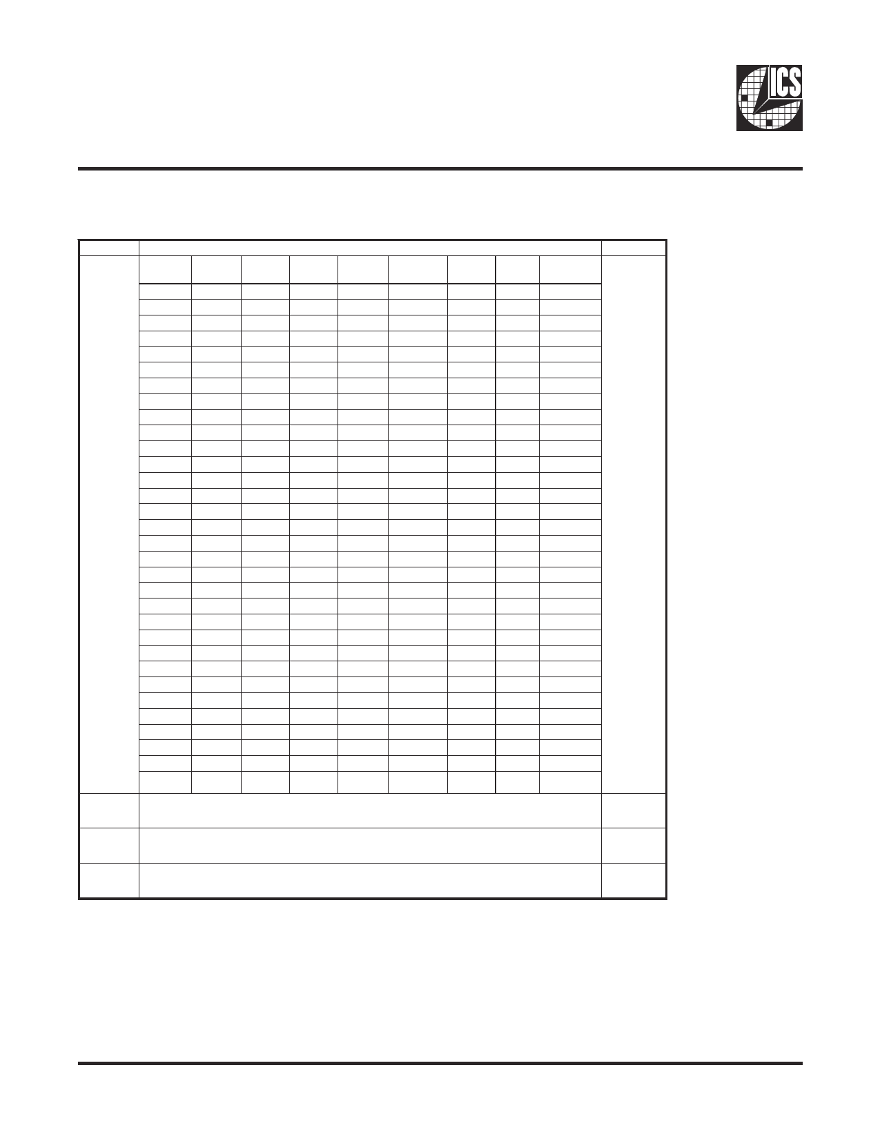
Serial Configuration Command Bitmap
Byte 0: Functionality and frequency select register (Default = 0)
Bit
Bit
(2, 7:4)
Bit 2
FS4
0
0
0
0
0
0
0
0
0
0
0
0
0
0
0
0
1
1
1
1
1
1
1
1
1
1
1
1
1
1
1
1
Bit 7
FS3
0
0
0
0
0
0
0
0
1
1
1
1
1
1
1
1
0
0
0
0
0
0
0
0
1
1
1
1
1
1
1
1
Bit 6
FS2
0
0
0
0
1
1
1
1
0
0
0
0
1
1
1
1
0
0
0
0
1
1
1
1
0
0
0
0
1
1
1
1
Bit 5
FS1
0
0
1
1
0
0
1
1
0
0
1
1
0
0
1
1
0
0
1
1
0
0
1
1
0
0
1
1
0
0
1
Description
Bit 4
FS0
CPU
0
103.0
1
100.0
0 100.45
1
100.9
0
107.1
1
109.0
0
112.0
1 114.00
0 116.00
1 118.00
0 133.30
1 120.00
0 122.00
1 125.00
0
50.0
1
66.7
0
133.3
1
133.9
0
138.0
1
142.0
0
146.0
1
150.0
0
153.0
1
156.0
0
159.1
1
162.0
0
166.7
1
168.0
0
171.0
1
174.0
0
177.0
1
1
180.0
PCI 3V66
34.33
33.33
33.48
33.63
35.70
36.33
37.33
28.50
29.00
29.50
33.33
30.00
30.50
31.25
16.67
16.67
33.33
33.48
34.50
35.50
36.50
37.50
38.25
39.00
39.78
40.50
41.67
42.00
42.75
43.50
44.25
45.00
68.67
66.67
66.97
67.27
71.40
72.67
74.67
57.00
58.00
59.00
66.65
60.00
61.00
62.50
33.33
33.33
66.67
66.95
69.00
71.00
73.00
75.00
76.50
78.00
79.55
81.00
83.33
84.00
85.50
87.00
88.50
90.00
Bit 3
0 - Frequency is selected by hardware select, latched inputs
1 - Frequency is selected by Bit 2, 7:4
Bit 1
0 - Normal
1 - Spread spectrum enabled
Bit 0
0 - Running
1 - Tristate all outputs
IOAPIC
17.17
16.67
16.74
16.82
17.85
18.17
18.67
14.25
14.50
14.75
16.66
15.00
15.25
15.63
8.33
8.33
16.67
16.74
17.25
17.75
18.25
18.75
19.13
19.50
19.89
20.25
20.83
21.00
21.38
21.75
22.13
22.50
PWD
Reserved
Note 1
0
1
0
Note 1:
Default at power-up will be for latched logic inputs to define frequency, as displayed byBit 3.
0600A—08/04/03
4
Share Link: