IPB09N03LAG 查看數據表(PDF) - Infineon Technologies
零件编号
产品描述 (功能)
生产厂家
IPB09N03LAG Datasheet PDF : 9 Pages
| |||
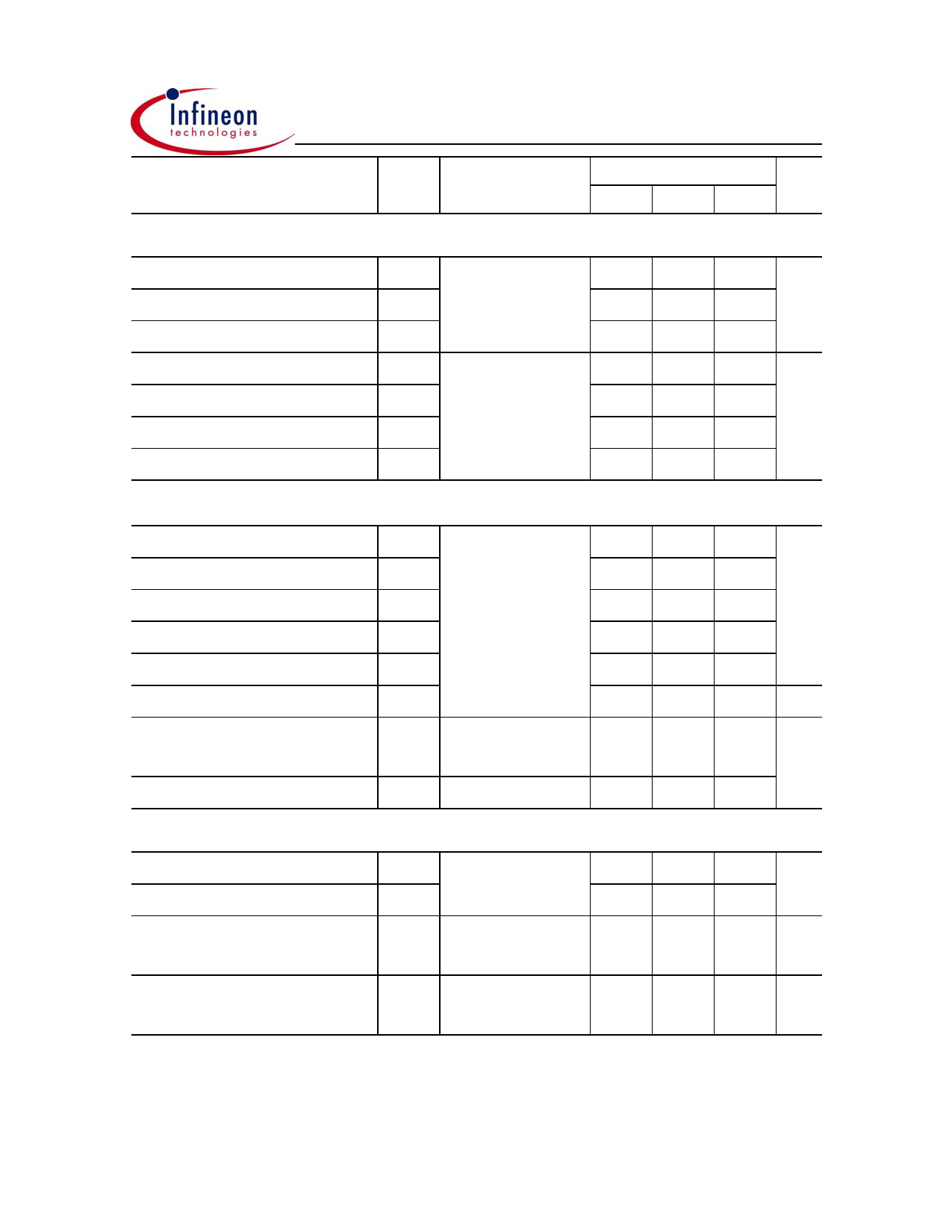
Parameter
Symbol Conditions
IPB09N03LA G
min.
Values
typ.
Unit
max.
Dynamic characteristics
Input capacitance
Output capacitance
Reverse transfer capacitance
Turn-on delay time
Rise time
Turn-off delay time
Fall time
Gate Charge Characteristics6)
Gate to source charge
Gate charge at threshold
Gate to drain charge
Switching charge
Gate charge total
Gate plateau voltage
Gate charge total, sync. FET
Output charge
C iss
-
C oss
V GS=0 V, V DS=15 V,
f =1 MHz
-
Crss
-
t d(on)
-
tr
V DD=15 V, V GS=10 V,
-
t d(off)
I D=25 A, R G=2.7 Ω
-
tf
-
1235
474
61
8.9
73
22
3.2
1642 pF
630
92
13 ns
109
33
4.8
Q gs
-
4.3
5.7 nC
Q g(th)
-
2.0
2.6
Q gd
V DD=15 V, I D=25 A,
-
2.8
4.3
Q sw
V GS=0 to 5 V
-
5.2
7.3
Qg
-
10
13
V plateau
-
3.5
-V
Q g(sync)
V DS=0.1 V,
V GS=0 to 5 V
-
8.7
12 nC
Q oss
V DD=15 V, V GS=0 V
-
10
14
Reverse Diode
Diode continous forward current
Diode pulse current
Diode forward voltage
Reverse recovery charge
IS
I S,pulse
T C=25 °C
V SD
V GS=0 V, I F=50 A,
T j=25 °C
Q rr
V R=15 V, I F=I S,
di F/dt =400 A/µs
-
-
50 A
-
-
350
-
0.99
1.2 V
-
-
10 nC
6) See figure 16 for gate charge parameter definition
Rev. 1.6
page 3
2006-05-11
Share Link: 