1766 查看數據表(PDF) - Linear Technology
零件编号
产品描述 (功能)
生产厂家
1766 Datasheet PDF : 30 Pages
| |||
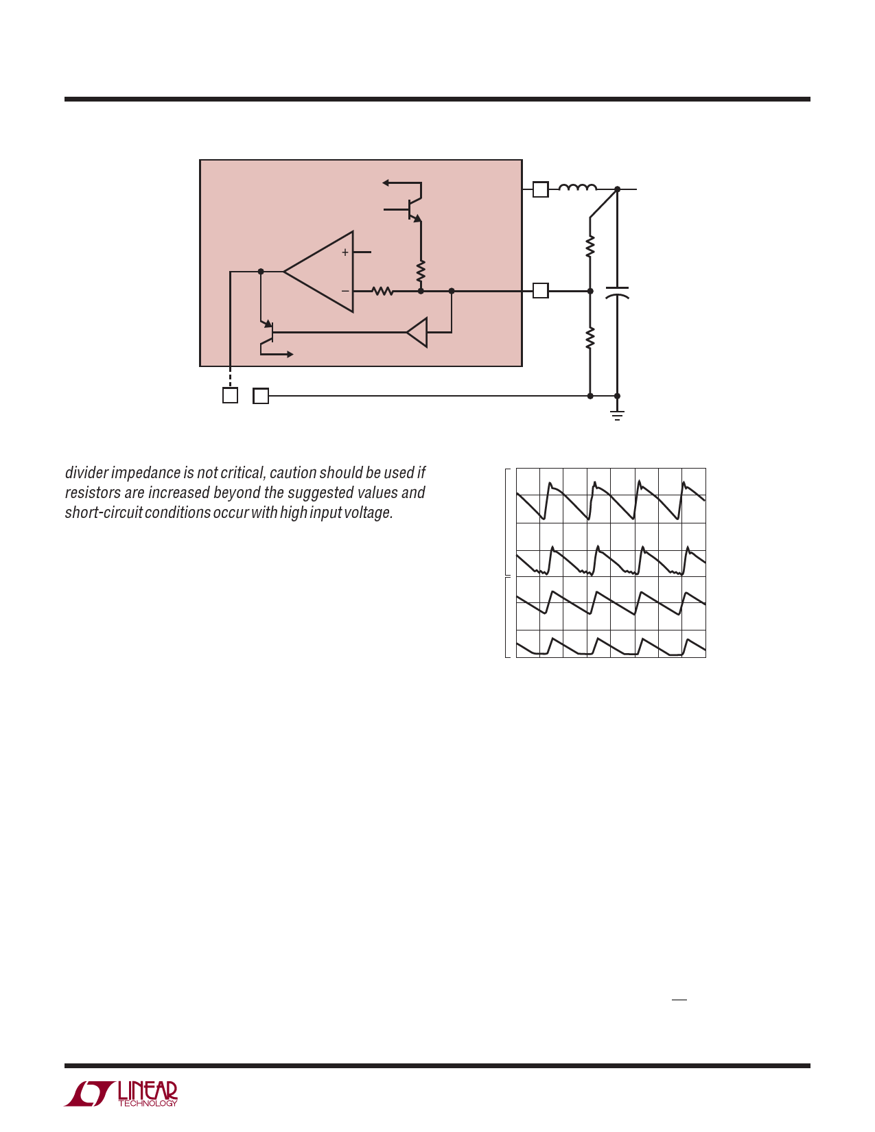
APPLICATIONS INFORMATION
LT1766
TO FREQUENCY
SHIFTING
ERROR
AMPLIFIER
1.4V
1.2V
R3
1k
Q1
R4
2k
BUFFER
Q2
TO SYNC CIRCUIT
LT1766/LT1766-5
VSW
L1
OUTPUT
5V
R1
FB
+
C1
R2
5k
VC GND
1766 F02
Figure 2. Frequency and Current Limit Foldback
divider impedance is not critical, caution should be used if
resistors are increased beyond the suggested values and
short-circuit conditions occur with high input voltage. High
frequency pickup will increase and the protection accorded
by frequency and current foldback will decrease.
40mV/DIV
VOUT AT IOUT = 1A
VOUT AT IOUT = 0.1A
CHOOSING THE INDUCTOR
For most applications, the output inductor will fall into
the range of 15μH to 100μH. Lower values are chosen to
reduce physical size of the inductor. Higher values allow
more output current because they reduce peak current
seen by the LT1766 switch, which has a 1.5A limit. Higher
values also reduce output ripple voltage.
When choosing an inductor you will need to consider
output ripple voltage, maximum load current, peak induc-
tor current and fault current in the inductor. In addition,
other factors such as core and copper losses, allowable
component height, EMI, saturation and cost should also
be considered. The following procedure is suggested
as a way of handling these somewhat complicated and
conflicting requirements.
Output Ripple Voltage
Figure 3 shows a typical output ripple voltage wave-
form for the LT1766. Ripple voltage is determined by
ripple current (ILP-P) through the inductor and the high
frequency impedance of the output capacitor. The fol-
lowing equations will help in choosing the required
0.5A/DIV
INDUCTOR CURRENT
AT IOUT = 1A
VIN = 40V
VOUT = 5V
L = 47μH
2.5μs/DIV
C = 100μF, 10V, 0.1Ω
INDUCTOR CURRENT
AT IOUT = 0.1A
1766 F03
Figure 3. LT1766 Ripple Voltage Waveform
inductor value to achieve a desirable output ripple volt-
age level. If output ripple voltage is of less importance,
the subsequent suggestions in Peak Inductor and Fault
Current and EMI will additionally help in the selection of
the inductor value.
Peak-to-peak output ripple voltage is the sum of a triwave
(created by peak-to-peak ripple current (ILP-P) times ESR)
and a square wave (created by parasitic inductance (ESL)
and ripple current slew rate). Capacitive reactance is as-
sumed to be small compared to ESR or ESL.
VRIPPLE
=
(ILP-P
)(ESR)
+
(ESL)
dI
dt
1766fc
11
Share Link: 