LT3570(RevA) 查看數據表(PDF) - Linear Technology
零件编号
产品描述 (功能)
生产厂家
LT3570 Datasheet PDF : 20 Pages
| |||
LT3570
APPLICATIONS INFORMATION
Boost Diode Selection
A Schottky diode is recommended for use with the LT3570
inverter/boost regulator. The Microsemi UPS120 is a very
good choice. Where the input to output voltage differen-
tial exceeds 20V, use the UPS140 (a 40V diode). These
diodes are rated to handle an average forward current of
1A. For applications where the average forward current
of the diode is less than 0.5A, use an ON Semiconductor
MBR0520L diode.
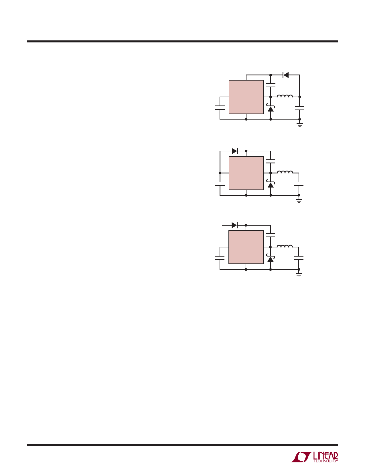
BOOST Pin Considerations
The capacitor and diode tied to the BOOST pin generate
a voltage that is higher than the input voltage. In most
cases, a 0.1μF capacitor and fast switching diode (such
as the CMDSH-3 or MMSD914LT1) will work well. Fig-
ure 2 shows three ways to arrange the boost circuit. The
BOOST pin must be more than 2.5V above the SW pin for
full efficiency. For outputs of 3.3V and higher, the standard
circuit (Figure 2a) is best. For outputs between 2.8V and
3.3V, use a small Schottky diode (such as the BAT-54).
For lower output voltages, the boost diode can be tied
to the input (Figure 2b). The circuit in Figure 2a is more
efficient because the BOOST pin current comes from a
lower voltage source. Finally, as shown in Figure 2c, the
anode of the boost diode can be tied to another source
that is at least 3V. For example, if you are generating 3.3V
and 1.8V and the 3.3V is on whenever the 1.8V is on, the
1.8V boost diode can be connected to the 3.3V output. In
any case, be sure that the maximum voltage at the BOOST
pin is less than 60V and the voltage difference between
the BOOST and SW2 pins is less than 25V.
The minimum operating voltage of an LT3570 application
is limited by the undervoltage lockout (2.5V) and by the
maximum duty cycle. The boost circuit also limits the
minimum input voltage for proper start-up. If the input
voltage ramps slowly, or the LT3570 turns on when the
output is already in regulation, the boost capacitor may
not be fully charged. Because the boost capacitor charges
with the energy stored in the inductor, the circuit will rely
on some minimum load current to get the boost circuit
running properly. This minimum load will depend on input
and output voltages, and on the arrangement of the boost
circuit. The minimum load current generally goes to zero
14
D3
BOOST
C3
LT3570
VIN
SW
GND
D2
C2
(2a)
D3
BOOST
C5
LT3570
VIN
SW
GND
D2
C2
(2b)
D3
VEXT
BOOST
C5
LT3570
VIN
SW
GND
D2
C2
(2c)
3570 F02
Figure 2. Boost Pin Configurations
once the circuit has started. Even without an output load
current, in many cases the discharged output capacitor will
present a load to the switcher that will allow it to start.
Switcher Frequency Compensation
The LT3570 uses current mode control to regulate the
output. This simplifies loop compensation. In particular, the
LT3570 does not depend on the ESR of the output capaci-
tor for stability so you are free to use ceramic capacitors
to achieve low output ripple and small circuit size.
To compensate the feedback loop of the LT3570, a series
resistor-capacitor network should be connected from
the VC pin to GND. For most applications, a capacitor in
the range of 500pF to 4.7nF will suffice. A good starting
value for the compensation capacitor, CC, is 1nF. The
3570fa
Share Link: 