LT3570(RevA) 查看數據表(PDF) - Linear Technology
零件编号
产品描述 (功能)
生产厂家
LT3570 Datasheet PDF : 20 Pages
| |||
LT3570
APPLICATIONS INFORMATION
will be enabled again going through a soft-start cycle.
Note: Overtemperature protection is intended to protect the
device during momentary overload conditions. Continuous
operation above the specified maximum operating junction
temperature may result in device degradation or failure.
to system ground at one location. Additionally, keep
the SW and BOOST nodes as small as possible. This is
implemented in the suggested layout of Figure 8 for the
QFN package which shows the topside metal from the
DC1106A demonstration board.
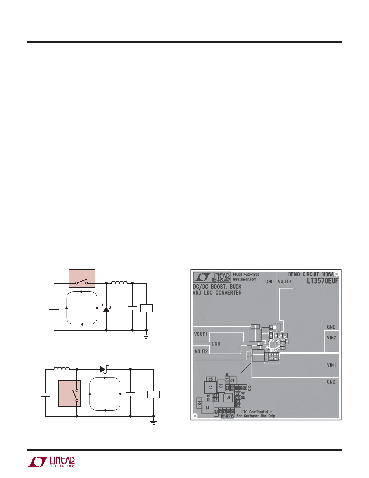
PCB Layout
For proper operation and minimum EMI, care must be
taken during printed circuit board (PCB) layout. Figure 6
shows the high current paths in the step-down regulator
circuit. Note that in the step-down regulator, large switched
currents flow in the power switch, the catch diode and the
input capacitor.
Figure 7 shows the high current paths in the step-up
regulator. In the boost regulator, large switched currents
flow through the power switch, the switching diode, and
the output capacitor.
The loop formed by these large switched current com-
ponents should be as small as possible. Place these
components on the same side of the circuit board and
connect them on that layer. Place a local, unbroken ground
plane below these components and tie this ground plane
Thermal Considerations
To deliver the power that the LT3570 is capable of, it
is imperative that a good thermal path be provided to
dissipate the heat generated within the package. This can
be accomplished by taking advantage of the large ther-
mal pad on the underside of the IC. It is recommended
that multiple vias in the printed circuit board be used to
conduct heat away from the IC and into a copper plane
with as much area as possible.
Related Linear Technology Publications
Application notes 19, 35, 44, 76 and 88 contain more
detailed descriptions and design information for buck
regulators and other switching regulators. The LT1375 data
sheet has a more extensive discussion of output ripple,
loop compensation, and stability testing.
LT3570
L2
HIGH
CIN
FREQUENCY
CIRCULATING
D1 COUT
LOAD
PATH
3570 F06
Figure 6. Buck High Speed Switching Path
L2
D1
LT3570
CIN
HIGH
FREQUENCY
SWITCHING
PATH
COUT LOAD
3750 F07
Figure 7. Boost High Speed Switching Path
Figure 8. Suggested Layout
3570fa
17
Share Link: 