MAX8566(2005) 查看數據表(PDF) - Maxim Integrated
零件编号
产品描述 (功能)
生产厂家
MAX8566 Datasheet PDF : 21 Pages
| |||
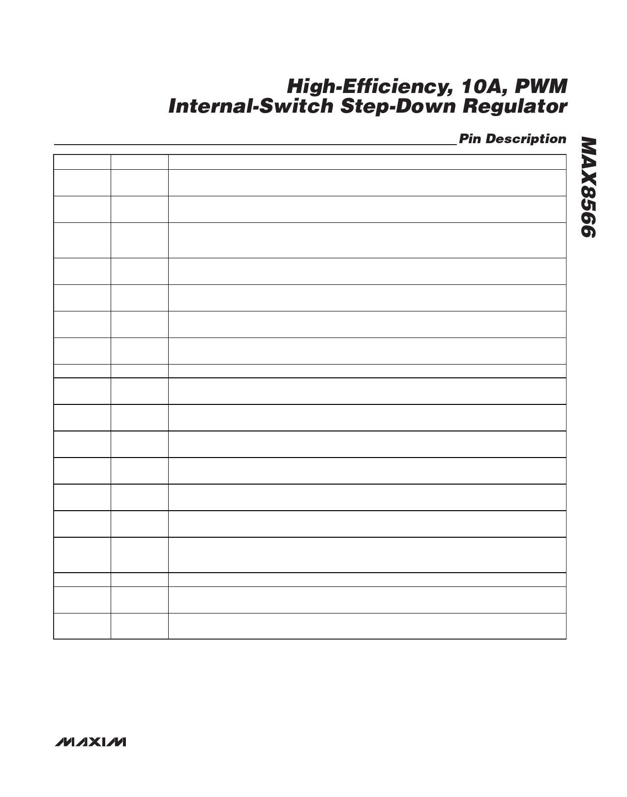
PIN
1
2
3
4
5–12
13–17
18–22
23
24
25
26
27
28
29
30
31
32
—
High-Efficiency, 10A, PWM
Internal-Switch Step-Down Regulator
Pin Description
NAME
MODE
FUNCTION
Monotonic Startup Enable/Disable. Connect MODE to GND or to the center tap of an external resistor-
divider to enable/disable monotonic startup mode.
COMP
Error-Amplifier Output. Connect the necessary compensation network from COMP to FB. COMP is
internally pulled to GND when the IC is in shutdown mode.
PWRGD
Power-Good Output. Open-drain output that is high impedance when VFB ≥ 90% of 0.6V. Otherwise,
PWRGD is internally pulled low. PWRGD is internally pulled low when the IC is in shutdown mode,
VDD is below the UVLO threshold, or the IC is in thermal shutdown.
BST
High-Side MOSFET Driver Supply. Bypass BST to LX with a 0.1µF capacitor. BST is connected to LSS
through an internal pMOS switch.
LX
Inductor Connection. All LX pins are internally connected together. Connect all LX pins to the
switched side of the inductor. LX is high impedance when the IC is in shutdown mode.
PGND
Power Ground. All PGND pins are internally connected. Connect all PGND pins externally to the
power ground plane.
IN
Input Power Supply. All IN pins are internally connected. Connect all IN pins externally to an input
supply from 2.3V to 3.6V. Bypass IN to PGND with 20µF of ceramic capacitance.
LSS
Low-Side MOSFET-Driver Supply Voltage. Connect to a 2.3V to 3.6V supply voltage.
VDD
IC Supply Voltage Input. Connect VDD to IN through an external 2Ω resistor. Bypass VDD to GND with
a 4.7µF capacitor.
REFIN
External Reference Input. Connect to an external reference. FB regulates to the voltage at REFIN.
Connect REFIN to SS to use the internal reference.
SS
Soft-Start Input. Connect a capacitor from SS to GND to set the soft-start time. See the Soft-Start
section.
EN
Enable Input. Active-high logic input to enable/disable the MAX8566. Connect to IN to enable the IC;
connect to GND to disable the IC.
SYNC
Synchronization Input. Synchronize to an external clock with a frequency of 250kHz to 2.4MHz. Leave
SYNC unconnected to disable the synchronization function.
FREQ
Oscillator Frequency Selection. Connect a resistor from FREQ to GND to select the switching
frequency. See the Frequency Select section.
SYNCOUT
GND
FB
EP
Oscillator Output. The SYNCOUT output is 180° out-of-phase from the internal oscillator or the SYNC signal
to facilitate running a second regulator 180° out-of-phase with the first to reduce input ripple current.
Analog Circuit Ground
Feedback Input. Connect to the center tap of an external resistor-divider from the output to GND to
set the output voltage.
Exposed Paddle. Connect to a large ground plane for increased thermal performance.
______________________________________________________________________________________ 11
Share Link: 