NB3N508S 查看數據表(PDF) - ON Semiconductor
零件编号
产品描述 (功能)
生产厂家
NB3N508S Datasheet PDF : 8 Pages
| |||
NB3N508S
Table 5. AC CHARACTERISTICS (VDD = 3.135 V to 3.465 V, GND = 0 V, TA = 0°C to +70°C, Note 7)
Symbol
Characteristic
Min
Typ
Max
Unit
fCLKIN
fCLKOUT
FNOISE
Crystal Input Frequency
Output Clock Frequency
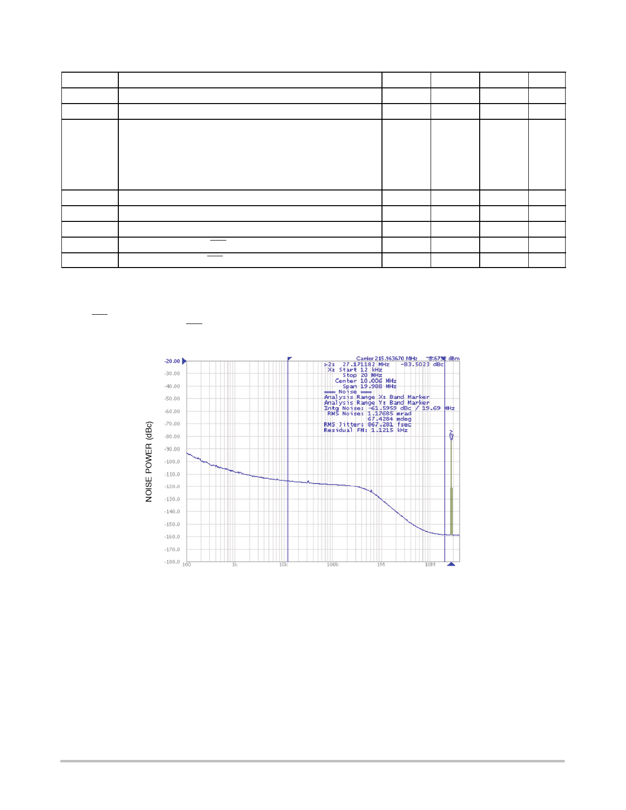
Phase−Noise Performance fCLKOUT = 216 MHz
@ 100 Hz Offset from Carrier
@ 1 kHz Offset from Carrier
@ 10 kHz Offset from Carrier
@ 100 kHz Offset from Carrier
@ 1 MHz Offset from Carrier
@ 10 MHz Offset from Carrier
27
216
−80
−88
−105
−106
−120
−145
MHz
MHz
dBc/Hz
Spurious Noise Components
−60
dBc/Hz
FP
tDUTY_CYCLE
tR
tF
Crystal Pullability 0 V v VIN v 3.3 V
Output Clock Duty Cycle (Measured at Crosspoint)
Output Rise Time (CLK/CLK) (Note 8)
Output Fall Time (CLK/CLK) (Note 8)
"100
45
50
380
380
ppm
55
%
500
ps
500
ps
NOTE: Device will meet the specifications after thermal equilibrium has been established when mounted in a test socket or printed circuit
board with maintained transverse airflow greater than 500 lfpm. Electrical parameters are guaranteed only over the declared
operating temperature range. Functional operation of the device exceeding these conditions is not implied. Device specification limit
values are applied individually under normal operating conditions and not valid simultaneously.
7. CLK/CLK loaded with 50 W receiver termination resistor between diff. pair.
8. Measured differentially (CLK − CLK) at 10% to 90%; RL = 50 W.
Phase Noise 10.00dB/Ref −20.00dBc/Hz
OFFSET FREQUENCY (Hz)
Figure 3. Typical Phase Noise Plot (VDD = 3.3 V, VIN = 0 V; Room Temperature)
http://onsemi.com
5
Share Link: 