LTC1196 查看數據表(PDF) - Linear Technology
零件编号
产品描述 (功能)
生产厂家
LTC1196 Datasheet PDF : 28 Pages
| |||
LTC1196/LTC1198
APPLICATIONS INFORMATION
OVERVIEW
The LTC1196/LTC1198 are 600ns sampling 8-bit A/D con-
verters packaged in tiny 8-pin SO packages and operating
on 3V to 6V supplies. The ADCs draw only 10mW from a
3V supply or 50mW from a 5V supply.
Both the LTC1196 and the LTC1198 contain an 8-bit,
switched-capacitor ADC, a sample-and-hold, and a serial
port (see Block Diagram). The on-chip sample-and-holds
have full-accuracy input bandwidths of 1MHz. Although
they share the same basic design, the LTC1196 and LTC1198
differ in some respects. The LTC1196 has a differential input
and has an external reference input pin. It can measure
signals floating on a DC common mode voltage and can
operate with reduced spans below 1V. The LTC1198 has a
2-channel input multiplexer and can convert either channel
with respect to ground or the difference between the two.
It also automatically powers down when not performing
conversion, drawing only leakage current.
SERIAL INTERFACE
The LTC1196/LTC1198 will interface via three or four wires
to ASICs, PLDs, microprocessors, DSPs, or shift registers
(see Operating Sequence in Figures 1 and 2). To run at their
fastest conversion rates (600ns), they must be clocked at
14.4MHz. HC logic families and any high speed ASIC or
PLD will easily interface to the ADCs at that speed (see
Data Transfer and Typical Application sections). Full speed
operation from a 3V supply can still be achieved with 3V
ASICs, PLDs or HC logic circuits.
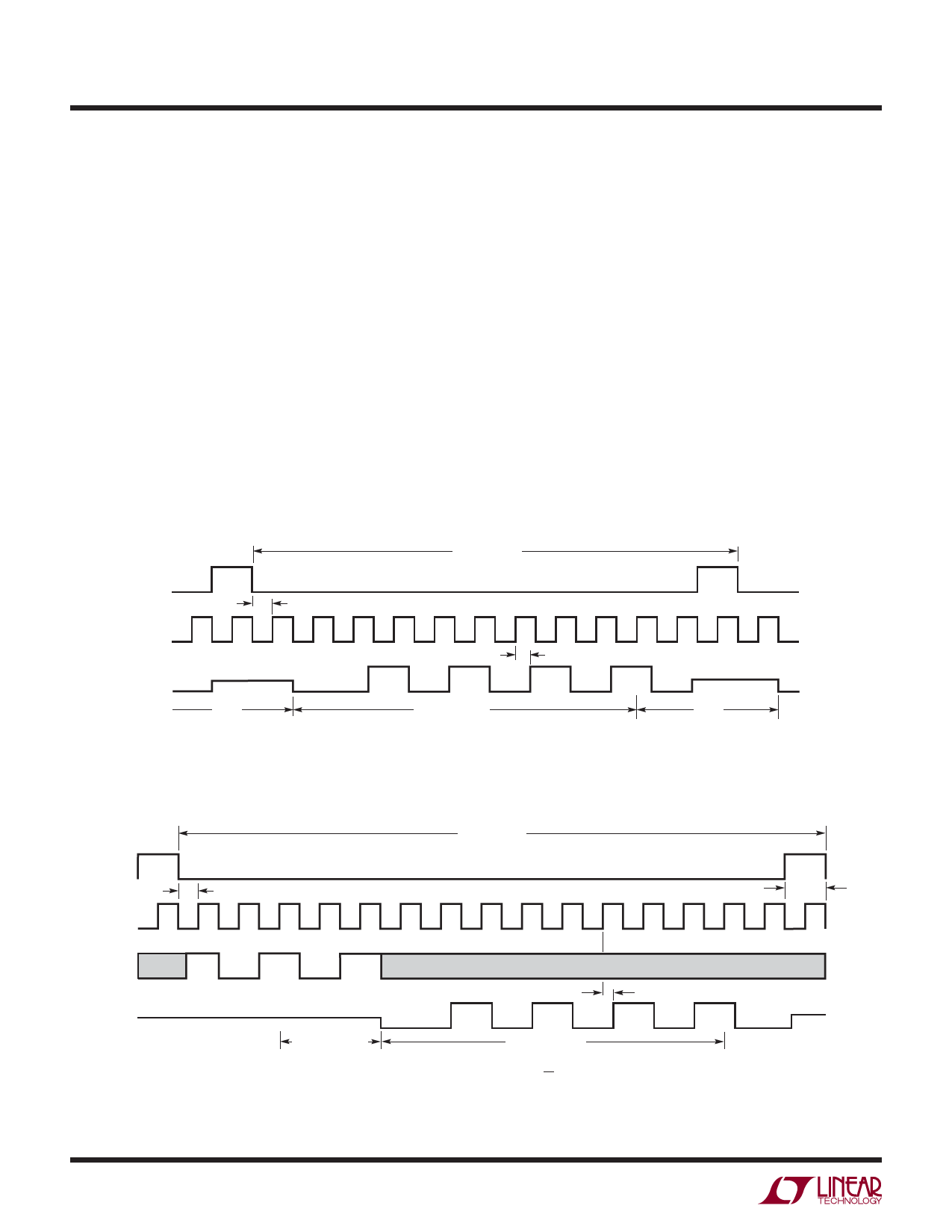
CS
tsuCS
tCYC (12 CLKs)
DOUT
B0
Hi-Z
tSMPL
tdDO
NULL BITS
B7
B6
B5
B4
B3
B2
B1
B0*
Hi-Z
tCYC (8.5 CLKs)
tSMPL
NULL
BITS
*AFTER COMPLETING THE DATA TRANSFER, IF FURTHER CLOCKS ARE APPLIED WITH CS LOW, THE ADC WILL OUTPUT ZEROS INDEFINITELY
1196/98 F01
Figure 1. LTC1196 Operating Sequence
CS
CLK
DIN
DOUT
tCYC (16 CLKs)
tsuCS
START
ODD/
SIGN
DUMMY
DON’T CARE
SGL/
DIFF
HI-Z
DUMMY
tdDO
NULL BITS
B7
B6
B5
B4
B3
B2
B1
tSMPL (2.5 CLKs)
tCONV (8.5 CLKs)
POWER
DOWN
Hi-Z
B0*
*AFTER COMPLETING THE DATA TRANSFER, IF FURTHER CLOCKS ARE APPLIED WITH CS LOW, THE ADC WILL OUTPUT ZEROS INDEFINITELY
1196/98 F02
Figure 2. LTC1198 Operating Sequence Example: Differential Inputs (CH1, CH0)
14
119698fa
Share Link: 