HI-6010 查看數據表(PDF) - Holt Integrated Circuits
零件编号
产品描述 (功能)
生产厂家
HI-6010 Datasheet PDF : 12 Pages
| |||
HI-6010
PIN 14 - RXD0 and PIN 16 - RXD1
receiver is not programmable to the 32 bit "extended buffer"
mode nor to the label recognition mode. Affecting the
receiver:
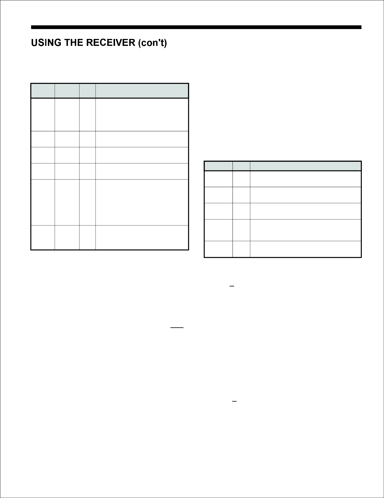
CONTROL PROGRAM PIN 5
BIT NAME VALUE VALUE
OPERATION
CR1
X
0 No action
0
1 No action
1
1 Next 8 data read cycles will read
stored labels. One time only sequence
on each transiton of CR1 to a 1.
CR2
0
X Receiver is disabled
1
X Receiver is enabled
CR3*
0
X RXRDY goes high normally
1
X Blocks RXRDY for one ARINC word
CR4
0
X Self test disabled
1
X Self test enabled
CR5
0
0 No parity errors enabled and 32nd
bit is data
1
0 Parity error flag enabled
0
1 32 bit "extended mode" enabled and
parity enabled.
1
1 8 bit "one byte at a time" mode and
parity enabled.
CR7
X
0 Label recognition not programmable
0
1 Label recognition disabled
1
1 Label recognition enabled
* CR3 will be automatically reset to 0 after being programmed
to a 1 at the completion of an ARINC word reception. This
allows a software label recognition different from the automatic
option available.
These pins must be 5 volt logic levels. There must be a
translator between the ARINC bus and these inputs.
Typically a receiver chip, such as the HI-8482 or HI-8588
is inserted between the ARINC bus and the logic chips.
RXD0 is looking for a high level for zero inputs and RXD1 is
looking for a high level for one inputs. When both inputs are
low this is referred to as the Null state.
SOFTWARE CONTROL OF THE RECEIVER
By writing to the Control Register and reading the Status
Register the controlling processor can operate the receiver
without hardware interrupts. The Control Register in
combination with the wiring of pin 5 was explained above.
The Status Register bits pertaining to the receiver are
explained below:
STATUS BIT VALUE
MEANING
SR1
0 No receiver data
1 Receiver data ready
SR3
0 No parity error
1 Parity error - Parity was even
SR4
0 Receiver data not overwritten
1 Receiver data was overwritten
SR5
0 Receiver data received without framing error
1 Framing error - Did not receive exactly 32
good bits
SR6
0 Did not receive first byte
1 Received first byte - Same flag as pin 13
COMMUNICATING WITH THE CONTROL AND
STATUS REGISTERS
PIN 6 - MR
When MR is a 1, the control word is set to 0X10 0101 (CR7 -
CR0). For the receiver this sets up 8 bit mode with the
receiver and parity enabled. MR also initializes the registers
and logic. The first ARINC reception will only occur after a
word gap.
PIN 8 - RXRDY
In 8 bit mode, this pin goes high whenever 8 bits are received
without error. In 32 bit mode this pin goes high after all 32 bits
are received with no error. This flag may be inhibited for one
ARINC word if CR3 is programmed to 1. This flag is also
inhibited in label recognition if the incoming ARINC label does
notmatch one of the stored 8 labels.
PIN 12 - RXC
This pin must have a clock applied that is 4X the desired
receive frequency.
PIN 13 - FCR
In 8 bit mode, this pin flags the first character (byte) received.
In 32 bit mode, this pin goes high for a valid 32 bit word. The
pin is not affected by CR3 programming.
Pin 27, C/D, must be high to read the status register or write
the control register. Reading the status register resets
errors. There is no provision to read the control register.
LABEL RECOGNITION OPTION
Pin 5 must be high if label recognition is selected in either the
8 or 32 bit modes and all eight label buffers must be written
using redundant labels, if necessary.
The chip compares the incoming label to the stored labels. If
a match is found, the data is processed. If a match is not
found, no indicators of receiving ARINC data are presented.
LOADING LABELS
After the write that changes CR7 from 0 to 1, the next 8 writes
of data (C/D is a zero for data) will load the label registers.
Labels must be loaded whenever pin 5 goes from low to
high.
READING LABELS
After the write that changes CR1 from 0 to 1, the next 8 data
reads are labels.
HOLT INTEGRATED CIRCUITS
4-5
Share Link: 