TDA1566 жҹҘзңӢж•ёж“ҡиЎЁпјҲPDFпјү - NXP Semiconductors.
йӣ¶д»¶зј–еҸ·
дә§е“ҒжҸҸиҝ° (еҠҹиғҪ)
з”ҹдә§еҺӮ家
TDA1566 Datasheet PDF : 46 Pages
| |||
NXP Semiconductors
TDA1566
I2C-bus controlled dual channel/single channel ampliп¬Ғer
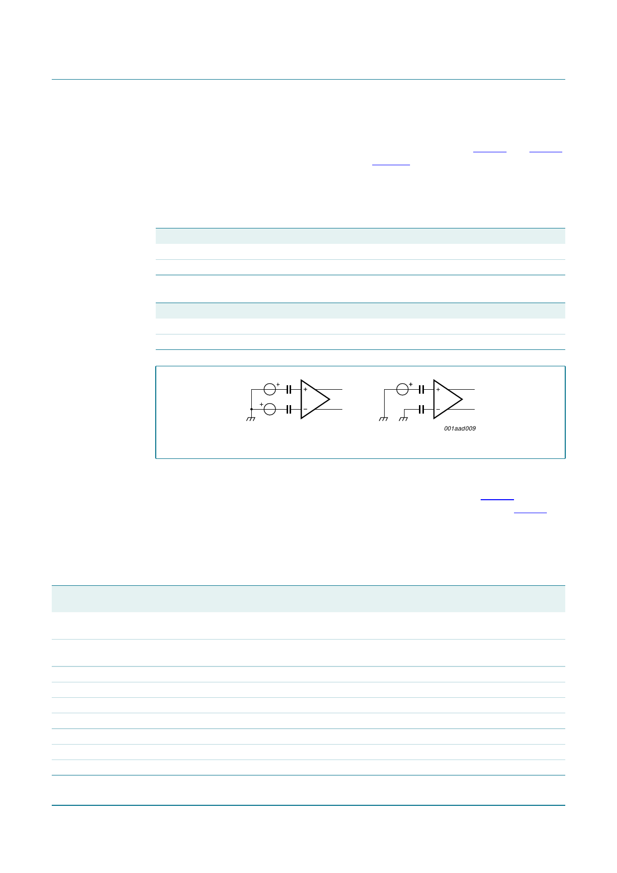
6.1.3 Balanced and unbalanced input sources
The TDA1566 accepts balanced as well as unbalanced input signals. Table 7 and Table 8
show the required hard or software setting and Figure 6 shows the input source
connection. Note that the unbalanced input source should be connected to the positive
BTL channel input. Note that the J version accepts in non-I2C-bus mode only a balanced
input source.
Table 7. Balanced and unbalanced input source setting TDA1566TH
Source
Balanced input source
Unbalanced input source
I2C-bus mode
IB3[D1] = 0
IB3[D1] = 1
Non-I2C-bus mode
ADS2 pin connected to GND ADS2 pin unconnected
Table 8. Balanced and unbalanced input source setting TDA1566J
Source
Balanced input source
Unbalanced input source
I2C-bus mode
IB3[D1] = 0
IB3[D1] = 1
Non-I2C-bus mode
default
not selectable
Fig 6. Balanced (left) and unbalanced (right) input source
001aad 009
6.1.4 Single channel 1 в„Ұ operation
The input and output pins for single channel 1 в„Ұ operation are listed in Table 9. The 1 в„Ұ
operation requires that on the PCB the output pins are shorted as indicated in Table 9. In
the 1 в„Ұ operation the input signal is taken from channel 1.
To prevent instability in 1 в„Ұ operation the ampliп¬Ғer must not be used in line driver mode
with a load larger than 25 в„Ұ.
Table 9.
Symbol
IN2+
IN2вҲ’
IN1+
IN1вҲ’
1OHM
OUT1+
OUT1вҲ’
OUT2+
OUT2вҲ’
Pinning for the single channel 1 в„Ұ mode; TDA1566TH and TDA1566J
Pin
Pin
Description single channel
(TDA1566TH) (TDA1566J) operation
Description dual channel
operation
2
22
disabled: connect IN2+ with 470 nF positive input channel 2
to SGND
3
23
disabled: connect IN2+ with 470 nF negative input channel 2
to SGND
10
3
positive input channel 1
positive input channel 1
11
4
negative input channel 1
negative input channel 1
15
8
1 в„Ұ select pin connected to VP
1 в„Ұ select pin connected to GND
16
10
positive output channel 1
positive output channel 1
18
13
negative output channel 1
negative output channel 1
19
15
shorted on board to OUT1вҲ’
positive output channel 2
21
18
shorted on board to OUT1+
negative output channel 2
TDA1566_2
Product data sheet
Rev. 02 вҖ” 20 August 2007
В© NXP B.V. 2007. All rights reserved.
9 of 46
Share Link: 