TS7514 查看數據表(PDF) - STMicroelectronics
零件编号
产品描述 (功能)
生产厂家
TS7514 Datasheet PDF : 19 Pages
| |||
TS7514
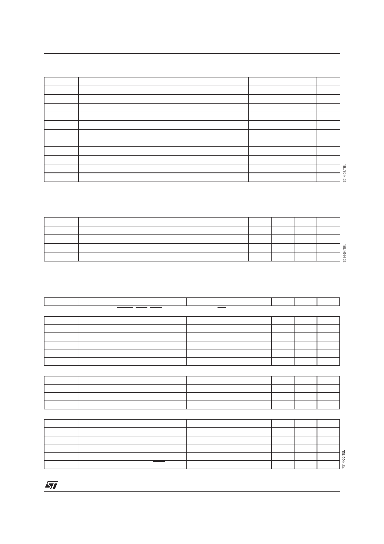
ABSOLUTE MAXIMUM RATINGS
Symbol
Parameter
Value
Unit
DGND DGND (digital ground) to AGND (analog ground)
– 0.3, + 0.3
V
V+
Supply Voltage V+ to DGND ro AGND
– 0.3, + 7
V
V–
Supply Voltage V- to DGND or AGND
– 7, + 0.3
V
VI
Voltage at any Digital Input
DGND - 0.3, V+ + 0.3
V
Vin
Io
Iout
Ptot
Top
Tstg
Tlead
Voltage at any Analog Input
Current at any Digital Output
Current at any Analog Output
Power Dissipation
Operating Temperature
Storage Temperature
Lead Temperature (soldering, 10s)
V– 0.3, V + + 0.3
V
– 20, + 20
mA
– 10, + 10
mA
500
mW
0, + 70
°C
– 65, + 150
°C
+ 260
°C
If the Maximum Ratings are exceeded, permanent damage may be caused to the device. This is a stress rating only, and functional operation
of the device under these or any other conditions for extended periods may affectdevice reliability. Standard CMOS handling procedures should
be employed to avoid possible damage to the device.
ELECTRIC OPERATING CHARACTERISTICS
Symbol
V+
V–
I+
I-
Positive Supply Voltage
Negative Supply Voltage
V+ Operating Current
V- Operating Current
Parameter
Min.
4.75
– 5.25
–
– 15
Typ.
5
– 5.0
10
– 10
Max.
5.25
– 4.75
15
–
Unit
V
V
mA
mA
DC AND OPERATING CHARACTERISTICS
Electrical characteristics are guaranteed over the complete temperature range, with typical load unless
otherwise specified. Typical values are given for : V+ = +5V, V− = -5V and room temperature = 25oC
Symbol
Parameter
Test Conditions
Min. Typ. Max. Unit
DIGITAL INTERFACE (MOD/DTMF, RTS, DCD, RxD, ZCO, TxD, MC/BC, ENP, PRD)
VI L
Input Voltage, Low Level
VI H
Input Voltage, High Level
II L
Input Current, Low Level
II H
Input Current, High Level
IOL
Output Current, Low Level
IOH
Output Current, High Level
ANALOG INTERFACE-PROGRAMMABLE (ATxl)
–
–
0.8
V
– 2.2
–
–
–
DGND < Vi < VIL (max) – 10
–
VIH (min) < VI < V+
– 10
–
10
µA
10
µA
VOL = 0.4V
1.6
–
–
mA
VOH = 2.8V
–
–
– 250 µA
Vin
Input Voltage Range
Iin
Input Current (filter output selected)
Cin
Input Capacitance (ATT output selected)
Rin
Input Resistance (ATT output selected)
– 1.8
–
+ 1.8
V
– 10
–
+ 10 µA
–
–
20
pF
100
–
–
kΩ
ANALOG INTERFACE - TRANSMIT OUTPUT (ATO) (load conditions RL = 560Ω, CL = 100pF)
VOS
Output Offset Voltage
CL
Load Capacitance
RL
Load Resistance
Vout
Output Voltage Swing
Ro ut
Output Resistance
–
ATO Attenuation Ratio when RTS = 1
– 250 – + 250 mV
–
–
100
pF
–
560
–
Ω
– 1.8
–
+ 1.8
V
10
–
25
Ω
70
–
–
dB
11/19
Share Link: 