UPD161831 查看數據表(PDF) - NEC => Renesas Technology
零件编号
产品描述 (功能)
生产厂家
UPD161831
NEC => Renesas Technology

UPD161831 Datasheet PDF : 67 Pages
| |||
µPD161831
Pin Symbol
Pin Name
MAS, /SLV Master slave control
Pin Name
449
V0-V4
γ -corrected power
supplies
525 to 516
VCOMH Amplitude voltage
536 to 539
COMC
COMDC
COMDCIN
COMDCSL
TCON
Square wave signal
542 to 546
output
Common center voltage 540, 541
output
Common center voltage 534, 535
external input
Common center voltage 533
external input switch
Timing generator
444
use/non-use selection
/RESET Reset
467
(2/2)
I/O
Description
Input
When the timing generator is used and 2 chips are connected in
cascade, selects use either as master IC or slave IC.
When the timing generator is not used, either leave this pin or input
a high level.
MAS, /SLV = L: Use as slave
MAS, /SLV = H: Use as master
Input
These pins input the γ -corrected power supplies from outside, the
relationship below must be observed. Also, be sure to stabilize the
gray-scale-level power supply during gray-scale voltage output.
VSS ≤ V4 ≤ V3 ≤ V2 ≤ V1 ≤ V0 ≤ VS
Output Outputs the voltage set with the amplitude voltage adjustment D/A
converter.
Output Outputs the square wave signal obtained through common
modulation of Vp-p voltage 0 V-VCOMH.
Output Outputs the common center voltage.
Input
Input
Input
Input
Input pin used to input the common center voltage from external.
Valid when COMDCSL = H.
Inputs a H level as the common voltage when the voltage input from
the COMDCIN pin is used.
This pin is used to select whether or not to use the timing generator.
TCON = L: Timing generator used
TCON = H: Timing generator not used
Reset pin. This is the active low signal.
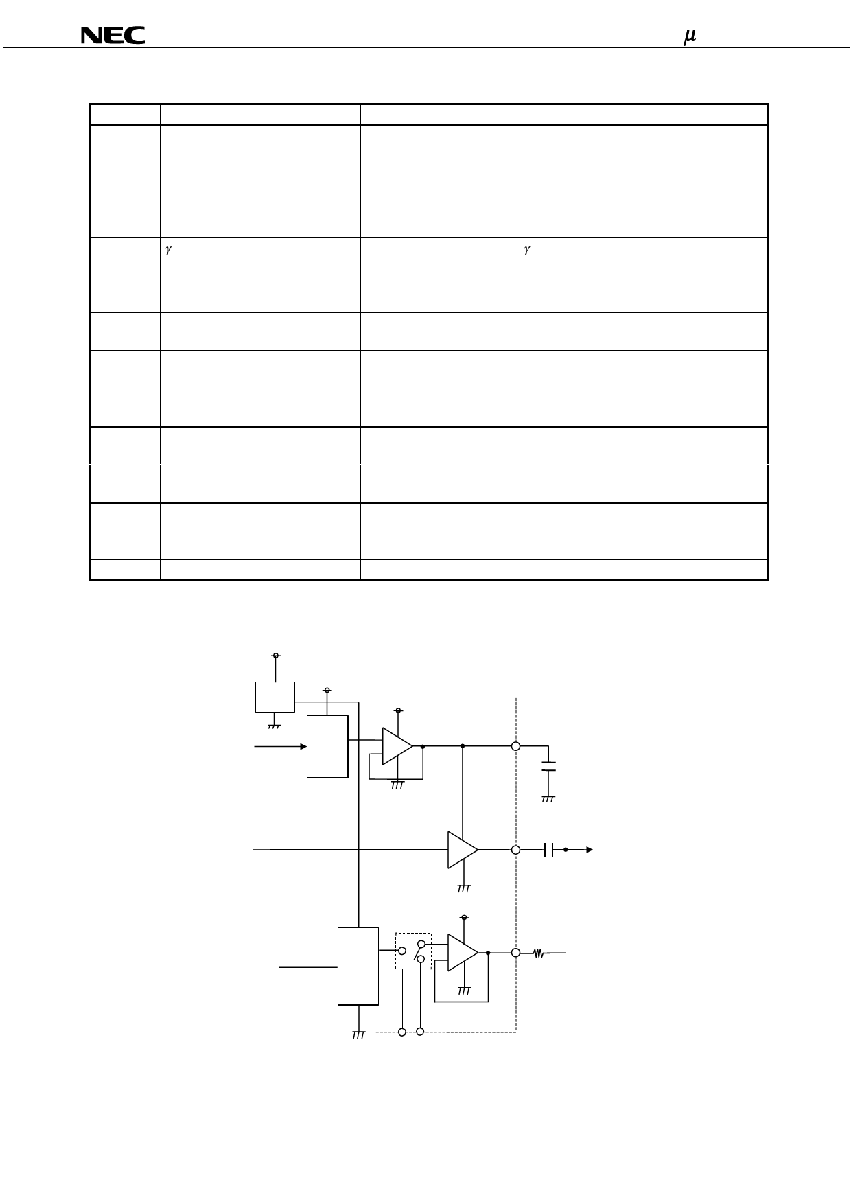
Figure 3−1. VCOM Application Example
VS
VS
R-strings
COMH (3:0)
register
4 bit DAC
R = 460 kΩ
to 920 kΩ
VS
(1/50) VS step
VCOMH [(34/50) VS to (49/50) VS]
4.7 µF
POL
COMM (6:0)
register
0.6 VS (V)
7 bit DAC
COMC
COM
VS
COMDC
COMDCSL COMDCIN
Preliminary Product Information S16269EJ2V0PM
7
Share Link: