HSP50016-EV 查看數據表(PDF) - Intersil
零件编号
产品描述 (功能)
生产厂家
HSP50016-EV Datasheet PDF : 18 Pages
| |||
HSP50016-EV
TABLE 5. SIGNAL MAPPING FOR CONNECTOR J1
PIN
NUMBER
J1A SIGNAL
MNEMONIC
J1B SIGNAL
MNEMONIC
1
N.C.
N.C.
2
PCD0 (D0)
N.C.
3
PCD1 (D1)
PCWR0 (INIT
PRINTER)
4
PCD2 (D2)
PCWR1 (SELECT
IN)
5
PCD3 (D3)
GND
6
PCD4 (D4)
GND
7
PCD5 (D5)
GND
8
PCD6 (D6)
GND
9
PCD7 (D7)
GND
10
N.C.
GND
11
PCRD0 (BUSY)
GND
12
PCRD2 (PAPER
GND
END)
13
PCRD1 (SELECT) GND
PCRD = PC Read; PCD = PC Data
TABLE 6. REGISTER TO INPUT/CONTROL BUS MAPPINGS
REGISTER
ADDRESS
DESTINATION
REGISTER
REGISTER
FUNCTION
0
U16
Clock and control
1
U11
DDC Control, TAP
2
U13
DDC Data input LS
Byte
3
U12
DDC Data Input MS
Byte
4-7
Not Used
N.C.
register. The On-Board Registers are down loaded by first
writing data to the Parallel Port Interface's Holding Register
U17 followed by two writes to the Address Register U18. By
writing the address register, data in the holding register is
loaded into one of the Registers U11, 12, 13, 16. The address
register specifies the particular register for loading as well as
the board address of the HSP50016-EV targeted for the data
download. The HSP50016-EV board address is selected by
placing a shorting jumper on one of the headers JP6-13 (see
Configuration Jumper Field Section), and the memory map for
the 8 data registers is shown in Table 6. The bit map for the
Parallel Port Interface’s Address Register is given in Table 7.
The Parallel Port Interface's Address and Holding Registers
are loaded with data from the PCD0-7 data lines of the
parallel port bus by a “low” to “high” transition on the
appropriate bus control line. Specifically, the address
register is loaded with data when a “low” to “high” transition
occurs on the PCWR0 line of the Parallel Port Bus, and the
holding register is loaded by a like transition on the PCWR1
line. The mapping of the parallel port bus signals to the PC's
parallel port is given in Table 5.
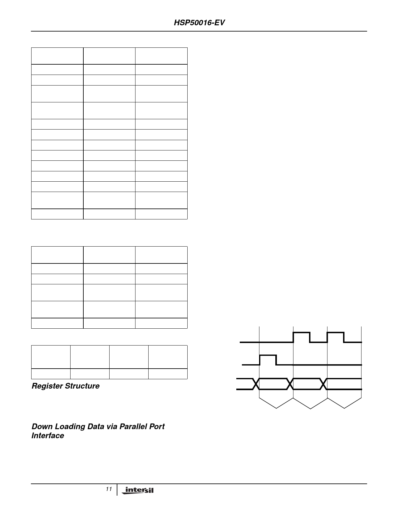
As an example, consider the loading of the least significant
byte of the data input, Register U13, as shown by the Timing
Diagram in Figure 7. First, data is down loaded to the
Parallel Port Interface's Holding Register. Next, the address
register is written with a value which contains the address of
U13 (see Table 6 for memory map), the HSP50016-EV
board address (assumed to be zero in this example), and a
“high” in the LD bit position (see Table 7 for Address Register
Bit Map). Finally, data is latched into the targeted register by
rewriting the address register with the same board and
register address but with a “low” in the LD bit position. The
“high/low” transition of the LD bit loads the data in the
holding register into the target data register on the specified
HSP50016-EV.
TABLE 7. ADDRESS REGISTER BIT MAP
NOT USED
LOAD
ADDRESS
RANGE
BOARD
ADDRESS
REGISTER
ADDRESS
D7
D6
D5-3
D2-0
Register Structure
The HSP50016-EV provides a set of registers which may be
used as a source for DDC input and control. They can be
loaded from either the parallel port or from the P1 connector.
Down Loading Data via Parallel Port
Interface
The control and input registers are down loaded from the PC
by a series of single byte writes to the to the Parallel Port
Interface. The Parallel Port Interface consists of two
decoders, an 8-bit address register, and an 8-bit holding
PCWR0
PCWR1
PCD0-7
DATA
0x42 (HEX)
0x02 (HEX)
DATA FOR
LSBYTE OF
DATA INPUT
WRITTEN TO
HOLDING REG
ADDRESS OF CODE TO TOG-
DATA INPUT GLE LOAD DATA
REG WRIT- LINE FOR U13
TEN TO
ADDRESS
REG
FIGURE 7. TIMING DIAGRAM FOR LOADING DATA INTO
LSBYTE OF DATA INPUT REGISTER
11
Share Link: 