VSC7217 查看數據表(PDF) - Vitesse Semiconductor
零件编号
产品描述 (功能)
生产厂家
VSC7217 Datasheet PDF : 36 Pages
| |||
VITESSE
SEMICONDUCTOR CORPORATION
Mutli-Gigabit Interconnect Chip
Preliminary Datasheet
VSC7217
General Description
The VSC7217 is a quad 8-bit parallel-to-serial and serial-to-parallel transceiver chip used for high band-
width interconnection between busses, backplanes, or other subsystems. Four Fibre Channel and Gigabit Ether-
net compliant transceivers provide up to 8.32Gb/s of duplex raw data transfer. Each channel can be operated at
a maximum data transfer rate of 1088Mb/s (8 bits at 136MHz) or a minimum rate of 784Mb/s (8 bits at
98MHz). For the entire chip in duplex mode, the aggregate transfer rate is between 6.3Gb/s and 8.7Gb/s. The
VSC7217 contains four 8B/10B encoders, serializers, de-serializers, 8B/10B decoders and elastic buffers which
provide the user with a simple interface for transferring data serially and recovering it on the receive side. The
device can also be configured to operate as four non-encoded 10-bit transceivers.
Notation
In this document, each of the four channels are identified as channel A, B, C or D. When discussing a signal
on any specific channel, the signal will have the channel letter embedded in the name: TA(7:0). When referring
to the common behavior of a signal which is used on each of the four channels, a lower case “n” is used in the
signal name: Tn(7:0). Differential signals, such as PTXA+ and PTXA-, may be referred to as a single signal,
PTXA, by dropping reference to the “+” and “-”. REFCLK refers either to the PECL/TTL input pair REF-
CLKP/REFCLKN, which can be differential PECL (using both REFCLKP and REFCLKN) or single-ended
TTL (using REFCLKP and leaving REFCLKN open).
Clock Synthesizer
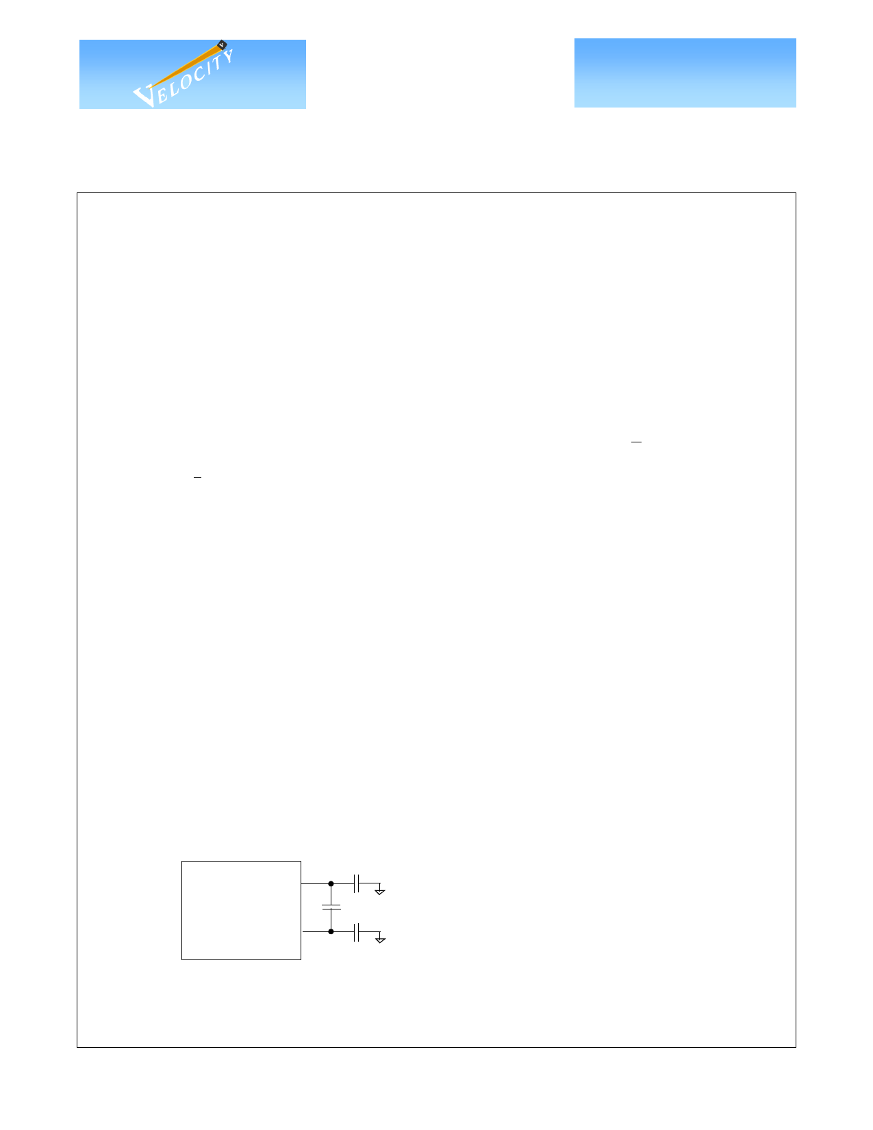
Depending on the state of the DUAL input, the VSC7217 clock synthesizer multiplies the reference fre-
quency provided on the REFCLK input by 10 (DUAL is LOW) or 20 (DUAL is HIGH) to achieve a baud rate
clock between 0.98GHz and 1.36 GHz. The on-chip Phase Lock Loop (PLL) uses a single external 0.1µF
capacitor, connected between CAP0 and CAP1, to control the Loop Filter. This capacitor should be a multilayer
ceramic dielectric, or better, with at least a 5V working voltage rating and a good temperature coefficient. NPO
is preferred but X7R may be acceptable. These capacitors are used to minimize the impact of common mode
noise on the Clock Multiplier Unit, especially power supply noise. Higher value capacitors provide better
robustness in systems. NPO is preferred because if an X7R capacitor is used, the power supply noise sensitivity
will vary with temperature. For best noise immunity, the designer may use a three capacitor circuit with one dif-
ferential capacitor between CAP0 and CAP1, C1, a capacitor from CAP0 to ground, C2, and a capacitor from
CAP1 to ground, C3 (Figure 1). Larger values are better but 0.1µF is adequate. However, if the designer cannot
use a three capacitor circuit, a single differential capacitor, C1, is adequate. These components should be iso-
lated from noisy traces.
Figure 1: Loop Filter Capacitors (Best Circuit)
C2
CAP0
C1
VSC7217
CAP1
C3
C1=C2=C3= >0.1uF
MultiLayer Ceramic
Surface Mount
NPO (Prefered) or X7R
5V Working Voltage Rating
The REFCLK signal can be either single-ended TTL or differential LVPECL. If TTL, connect the TTL
input to REFCLKP but leave REFCLKN open. If LVPECL, connect the inputs to REFCLKP and REF-
CLKN. Internal biasing resistors sets the proper DC Level to VDD/2.
Page 2
© VITESSE SEMICONDUCTOR CORPORATION
741 Calle Plano, Camarillo, CA 93012 • 805/388-3700 • FAX: 805/987-5896
G52325-0, Rev. 3.0
6/14/00
Share Link: 