VSC835UB 查看數據表(PDF) - Vitesse Semiconductor
零件编号
产品描述 (功能)
生产厂家
VSC835UB Datasheet PDF : 18 Pages
| |||
VITESSE
SEMICONDUCTOR CORPORATION
2.5 Gbits/sec
34x34 Crosspoint Switch with Signal Detection
Datasheet
VSC835
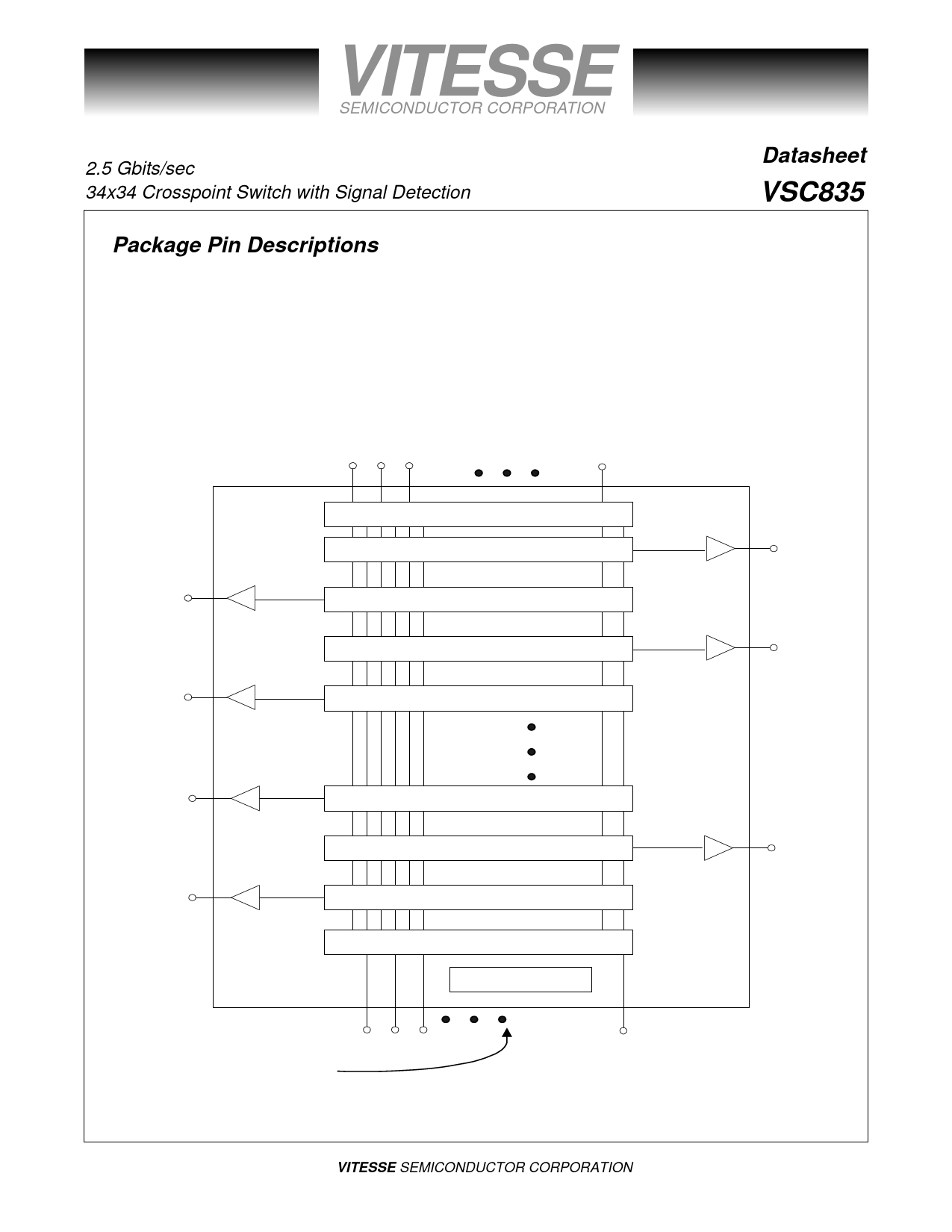
Package Pin Descriptions
The VSC835 is packaged in a 27x27mm 256 pin ball grid array package. The 256 BGA package is ther-
mally enhanced and carries the high-speed signals over controlled impedance lines from the solder ball to the
circuit die. The following sections describe the pinout and mechanical details of the VSC835.
Figure 6: Functional Pinout Floorplan
A0 A2 A4
A32
I/P LOS and termination
34:1 Switch slice
Y0
Y1
34:1 Switch slice
34:1 Switch slice
Y2
Y3
34:1 Switch slice
Y31
34:1 Switch slice
34:1 Switch slice
Y32
Y33
34:1 Switch slice
I/P LOS and termination
control logic
A1 A3 A5
A33
Programming
interface
Page 10
© VITESSE SEMICONDUCTOR CORPORATION
741 Calle Plano, Camarillo, CA 93012 • 805/388-3700 • FAX: 805/987-5896
G52270-0, Rev. 4.1
7/24/00
Share Link: 