VSC8150 查看數據表(PDF) - Vitesse Semiconductor
零件编号
产品描述 (功能)
生产厂家
VSC8150 Datasheet PDF : 20 Pages
| |||
VITESSE
SEMICONDUCTOR CORPORATION
Preliminary Data Sheet
VSC8150
2.488Gb/s SONET/SDH
Overhead Monitor
Table 8: Framing and B1 Error Output Timing (STS-3/STM-1 Mode)
Parameter
Description
Min
TFPW
Frame Pulse Width
—
TFERRSU
Frame Boundary Error delay with respect to RXFPOUT
—
TFERRPW
Frame Boundary Error pulse width high
—
TSEFSU
SEF transition delay time with respect to RXFPOUT
—
TB1SU
B1 Pulse train delay with respect to RXFPOUT
—
TB1PWH
B1 error pulse width high
—
TB1PWL
B1 error pulse width low
—
Note: Generated Waveforms are synchronous and assume a 155MHz RXSCLKIN signal.
Typ
51.4
0
51.4
103
13.96
409
409
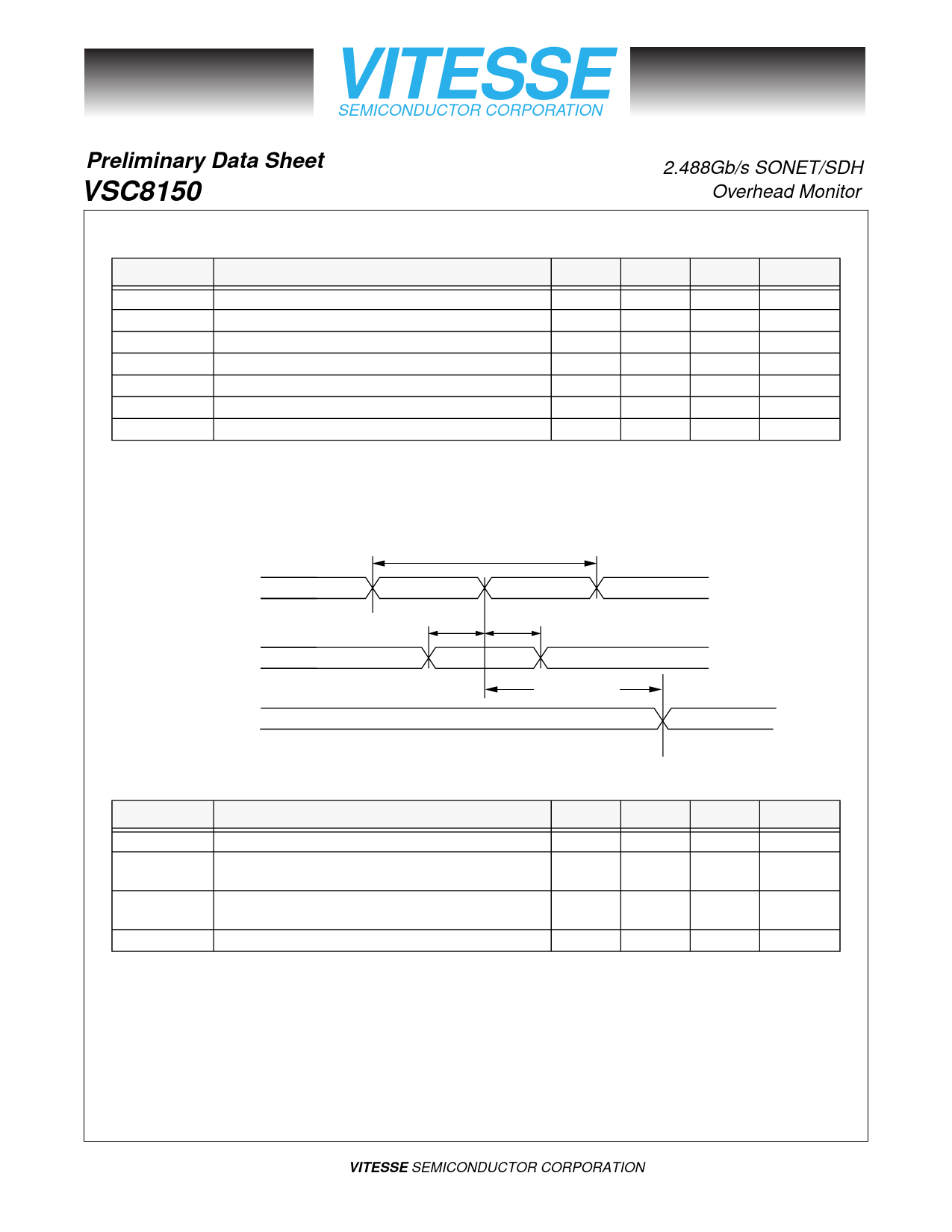
Figure 11: Serial Data Input Timing Diagram
Max
—
—
—
—
—
—
—
Units
ns
ns
ns
ns
µs
ns
ns
RXSCLKIN-
RXSCLKIN+
RXSIN+
RXSIN-
RXSLBOUT+
RXSLBOUT-
TRXSCLKIN
TRXSSU TRXSH
TRXSLBOUT
Table 9: Serial Data Input Timing
Parameter
Description
Min
Typ
Max
Units
TRXSCLKIN Serial Receive clock period
401.9
-
-
ps
TRXSSU
Serial Receive input data RXSIN setup time with respect
to falling edge of RXSCLKIN+
100
-
-
ps
TRXSH
Serial Receive input data RXSIN hold time with respect
to falling edge of RXSCLKIN+
75
-
-
ps
TRXSLBOUT Propagation delay from falling edge of RXSCLKIN+
430
-
820
ps
G52186-0, Rev. 3.0
10/12/98
© VITESSE SEMICONDUCTOR CORPORATION
741 Calle Plano, Camarillo, CA 93012 • 805/388-3700 • FAX: 805/987-5896
Page 11
Share Link: 