WED2ZL361MV 查看數據表(PDF) - White Electronic Designs Corporation
零件编号
产品描述 (功能)
生产厂家
WED2ZL361MV Datasheet PDF : 12 Pages
| |||
White Electronic Designs
WED2ZL361MV
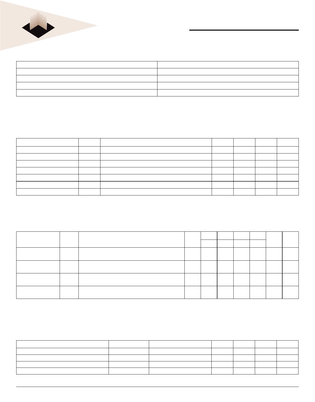
Absolute Maximum Ratings*
Voltage on VCC Supply Relative to VSS
VIN (DQx)
VIN (Inputs)
Storage Temperature (BGA)
Short Circuit Output Current
-0.3V to +4.6V
-0.3V to +4.6V
-0.3V to +4.6V
-65°C to +150°C
100mA
* Stress greater than those listed under “Absolute Maximum Ratings: may cause permanent damage to the device. This is a stress rating only and functional operation of the device at
these or any other conditions greater than those indicated in the operational sections of this specification is not implied. Exposure to absolute maximum rating condtions for extended
periods may affect reliability.
Recommended DC Operating Conditions Voltage Referenced to:
VSS = 0V, = 0°C ≤ TA ≤ +70°C; Commercial or -40°C ≤ TA ≤ +85°C; Industrial
Description
Input High (Logic 1) Voltage
Input Low (Logic 0) Voltage
Input Leakage Current
Output Leakage Current
Output High Voltage
Output Low Voltage
Supply Voltage
Symbol
VIH
VIL
ILI
ILO
VOH
VOL
VCC
Conditions
0V ≤ VIN ≤ VCC
Output(s) Disabled, 0V ≤ VIN ≤ VCC
IOH = -4.0mA
IOL = 8.0mA
Min
2.0
-0.3
-5
-5
2.4
–
3.135
Max
VCC +0.5
0.8
5
5
–
0.4
3.465
NOTES:
1. All voltages referenced to VSS (GND)
2. ZZ pin has an internal pull-up, and input leakage = ± 10µA.
Units
V
V
µA
µA
V
V
V
Notes
1
1
2
1
1
1
DC Characteristics
166 150 133 100
Description
Symbol Conditions
Typ MHz MHz MHz MHz Units Notes
Power Supply
Current: Operating
Power Supply
Current: Standby
Power Supply
Current: Current
Clock Running
Standby Current
IDD Device Selected; All Inputs ≤ VIL or ≥ VIH; Cycle Time =
TCYC MIN; VCC = MAX; Output Open
840 800 760 640 mA 1, 2
ISB2 Device Deselected; VCC = MAX; All Inputs ≤ VSS + 0.2 or 30
60
60
60
60
mA
2
VCC - 0.2; All Inputs Static; CLK Frequency = 0; ZZ ≤ VIL
ISB3 Device Selected; All Inputs ≤ VIL or ≥ VIH; Cycle Time =
30 60 60
60 60 mA
2
TCYC MIN; VCC = MAX; Output Open; ZZ ≥ VCC - 0.2V
ISB4 Device Deselected; VCC = MAX; All Inputs ≤ VSS + 0.2 or
VCC - 0.2; Cycle Time = TCYC MIN; ZZ ≤ VIL
240 220 180 160 mA 2
NOTES:
1. IDD is specified with no output current and increases with faster cycle times.
IDD increases with faster cycle times and greater output loading.
2. Typical values are measured at 3.3V, 25°C, and 10ns cycle time.
Description
Control Input Capacitance
Input/Output Capacitance (DQ)
Address Capacitance
Clock Capacitance
NOTES: 1. This parameter is sampled.
June 2004
Rev. 3
BGA Capacitance
Symbol
CI
CO
CA
CCK
Conditions
TA = 25°C; f = 1MHz
TA = 25°C; f = 1MHz
TA = 25°C; f = 1MHz
TA = 25°C; f = 1MHz
Typ
Max
Units Notes
5
7
pF
1
6
8
pF
1
5
7
pF
1
3
5
pF
1
4
White Electronic Designs Corporation • (602) 437-1520 • www.wedc.com
Share Link: 