ICM7231 查看數據表(PDF) - Intersil
零件编号
产品描述 (功能)
生产厂家
ICM7231 Datasheet PDF : 16 Pages
| |||
ICM7231, ICM7232
OPEN
200kΩ
2 VDISP 40
+5
10nF
36
ICM7231
ICM7232
FIGURE 10. SIMPLE DISPLAY VOLTAGE ADJUSTMENT
Figure 11A shows another method of setting up a display
voltage using five silicon diodes in series. These diodes,
1N914 or equivalent, will each have a forward drop of
approximately 0.65V, with approximately 20µA flowing
through them at room temperature. Thus, 5 diodes will give
3.25V, suitable for a 3V display using the material properties
shown in Figures 4 and 5. For higher voltage displays, more
diodes may be added. This circuit provides reasonable
temperature compensation, as each diode has a negative
temperature coefficient of -2mV/oC; five in series gives
-10mV/oC, not far from optimum for the material described.
The disadvantage of the diodes in series is that only integral
multiples of the diode voltage can be achieved. The diode
voltage multiplier circuit shown in Figure 11B allows fine-
tuning the display voltage by means of the potentiometer; it
likewise provides temperature compensation since the tem-
perature coefficient of the transistor base-emitter junction
(about -2mV/oC) is also multipled. The transistor should have
a beta of at least 100 with a collector current of 10µA. The
inexpensive 2N2222 shown in the figure is a suitable device.
VDD
1N914
DIODES
40kΩ
2 VDISP 40
+5
36
ICM7231
ICM7232
10nF
FIGURE 11A. STRING OF DIODES
VDD
200kΩ
POTENTIOMETER
2N2222
2 VDISP 40
+5
36
ICM7231
ICM7232
40kΩ
10nF
FIGURE 11B. TRANSISTOR-MULTIPLIER
FIGURE 11. DIODE-BASED TEMPERATURE COMPENSATION
For battery operation, where the display voltage is generally the
same as the battery voltage (usually 3 - 4.5V), the chip may be
operated at the display voltage, with VDlSP connected to VSS.
The inputs of the chip are designed such that they may be
driven above VDD without damaging the chip. This allows, for
example, the chip and display to operate at a regulated 3V, and
a microprocessor driving its inputs to operate with a less well
controlled 5V supply. (The inputs should not be driven more
than 6.5V above GND under any circumstances.) This also
allows temperature compensation with the ICL7663S, as
shown in Figure 12. This circuit allows independent adjustment
of both voltage and temperature compensation.
+5V
LOGIC
SYSTEM
PROCESSOR,
ETC.
VIN +
VOUT1
VOUT2
1.8MΩ
ICL7663S
VSET
VTC
GND
300kΩ
2.7MΩ
VDD
ICM7233
VDISP
GND
DATA BUS
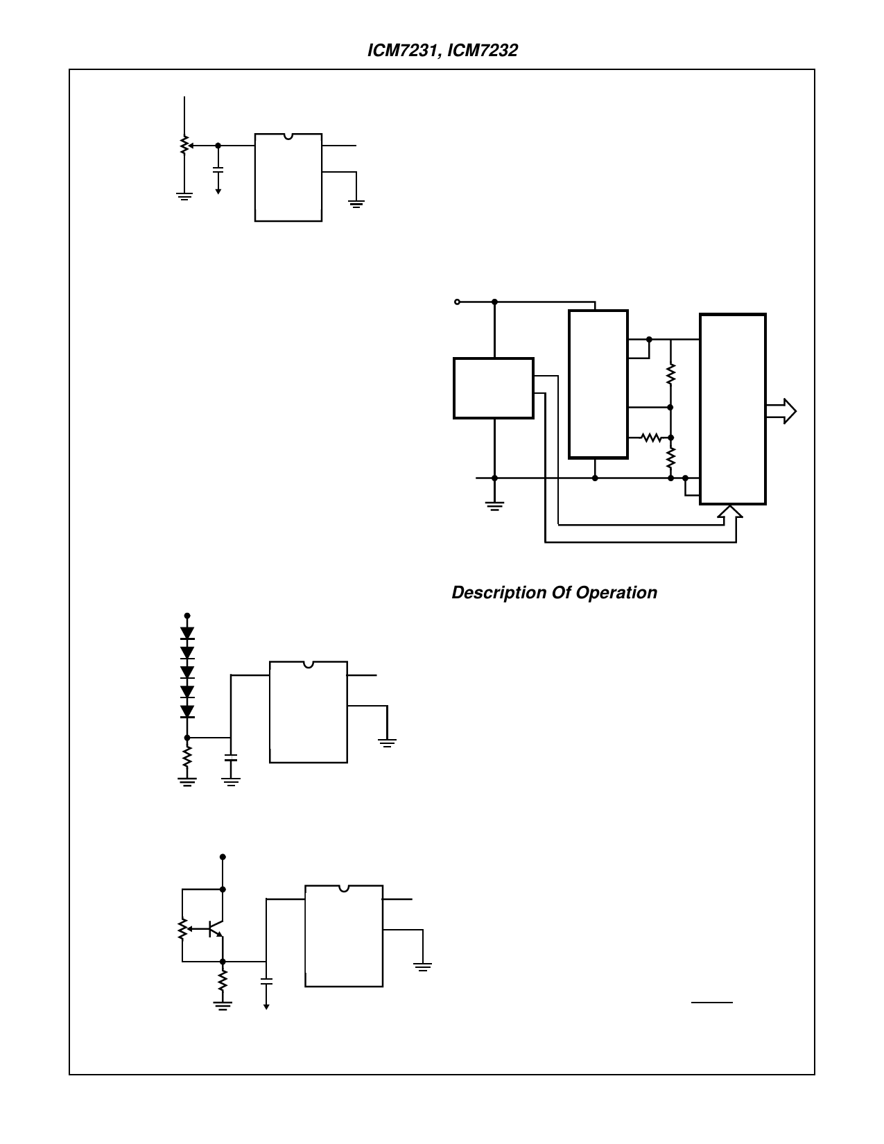
FIGURE 12. FLEXIBLE TEMPERATURE COMPENSATION
Description Of Operation
Parallel Input Of Data And Address (ICM7231)
The parallel input structure of the ICM7231 device is
organized to allow simple, direct interfacing to all micropro-
cessors, (see the Functional Block Diagram). In the
ICM7231, address and data bits are written into the input
latches on the rising edge of the Chip Select input.
The rising edge of the Chip Select also triggers an on-chip
pulse which enables the address decoder and latches the
decoded data into the addressed digit/character outputs. The
timing requirements for the parallel input device are shown in
Figure 1, with the values for setup, hold, and pulse width times
shown in the AC Specifications section. Note that there is a
minimum time between Chip Select pulses; this is to allow suf-
ficient time for the on-chip enable pulse to decay, and ensures
that new data doesn’t appear at the decoder inputs before the
decoded data is written to the outputs.
Serial Input Of Data And Address (ICM7232)
The ICM3232 trades six pins used as data inputs on the
ICM7231 for six more segment lines, allowing two more
9-segment digits. This is done at the cost of ease in interfac-
ing, and requires that data and address information be
entered serially. Refer to Functional Block Diagram and tim-
ing diagrams, Figures 2 and 3. The interface consists of four
pins: DATA Input, DATA CLOCK Input, WRITE Input and
DATA ACCEPTED Output. The data present at the DATA
Input is clocked into a shift register on the rising edge of the
9-29
Share Link: 