SIW3500GIG1 查看數據表(PDF) - RF Micro Devices
零件编号
产品描述 (功能)
生产厂家
SIW3500GIG1 Datasheet PDF : 18 Pages
| |||
Preliminary
SiW3500
Pin Description
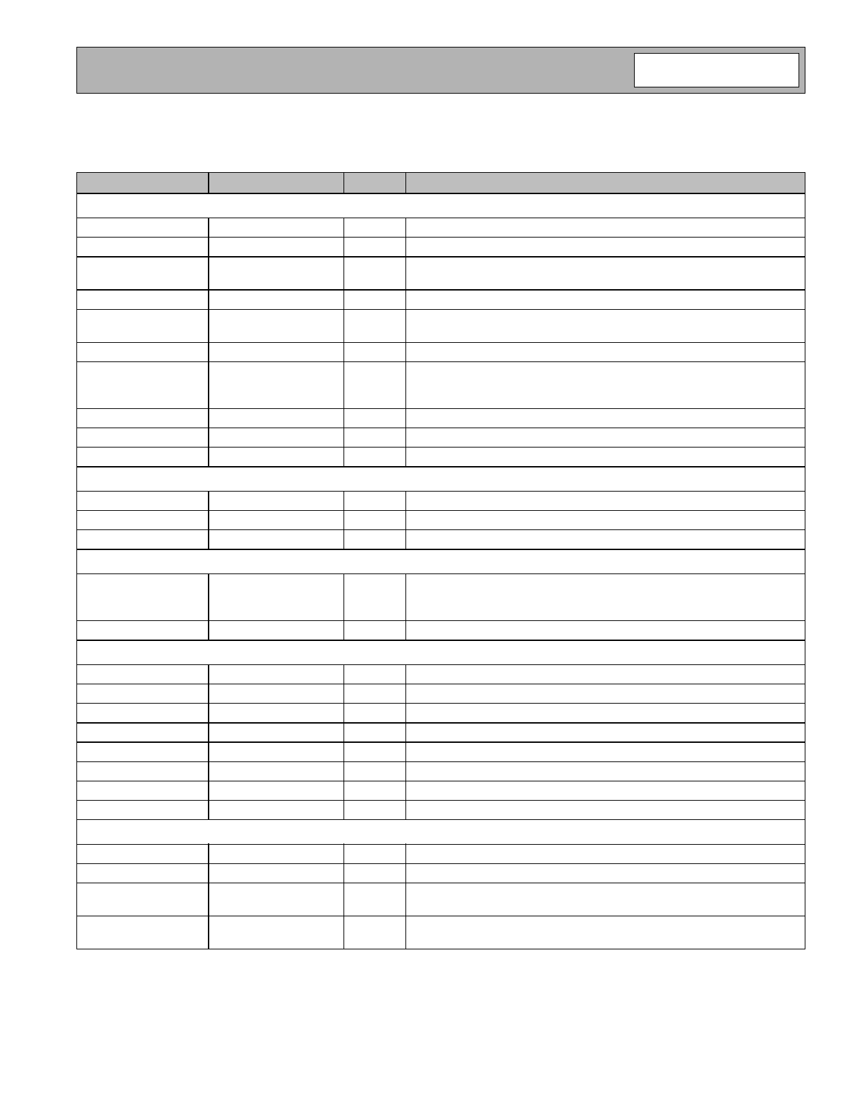
The following table provides detailed listings of pin descriptions arranged by functional groupings.
Name
Pad Type
Ball
Description
Radio (Power from VCC)
RF_IO
Analog
TX_BIAS
Analog
VTUNE
Analog
CHG_PUMP
Analog
XTAL_N
Analog
XTAL_P/CLK
Analog
IDAC
Analog
ADC_IN
VREFN_CAP
VREFP_CAP
Analog
Analog
Analog
A2
RF signal. Input and output.
A4
Internal transmitter driver bias.
A6
Pin for reference PLL loop filter, only used if reference frequency is not
integer multiples of 4 MHz.
F1
Pin for RF loop filter.
B7
System clock crystal negative input. If a reference clock is used, this pin
should be left unconnected.
A7
System clock crystal positive input or reference clock input.
Power control to external power amplifier. This output provides a variable
B1
current source that can be used to control the external power amp. Leave
unconnected if not used.
J2
Analog to digital converter input or FREQ_SEL_(0).
C2
Decoupling capacitor for internal A/D converter voltage reference.
C1
Decoupling capacitor for internal A/D converter voltage reference.
Low Power Oscillator and Reset (Power from VDD_P_ALT)
CLK32K_IN
Analog
L1
For crystal or external clock input (32.768 kHz).
CLK32K_OUT
Analog
K1
Drive for crystal.
RESET_N
CMOS input
G1
System level reset (active low).
Power Control Interface (Power from VDD_P)
PWR_REG_EN
CMOS bi-directional G2
AUX_TXD
CMOS bi-directional G9
CLOCK_REQ_OUT control line for external TCXO by default, or can be
used as enable for an external voltage regulator. Programmable active
high or active low.
Auxiliary UART serial port output.
Multi-function (MFP) I/O (Power from VDD_P)
MFP [0]
CMOS bi-directional F3
MFP [1]
CMOS bi-directional J1
MFP [2]
CMOS bi-directional L6
MFP [3]
CMOS bi-directional F10
MFP [4]
CMOS bi-directional B9
MFP [5]
CMOS bi-directional C8
MFP [6]
CMOS bi-directional C7
MFP [7]
CMOS bi-directional C6
Multi-function I/O port.
Multi-function I/O port.
Multi-function I/O port.
Multi-function I/O port.
Multi-function I/O port.
Multi-function I/O port.
Multi-function I/O port.
Multi-function I/O port.
PCM Interface (Power from VDD_P_ALT)
PCM_IN
CMOS bi-directional H3
PCM_OUT
CMOS bi-directional L2
PCM_CLK
CMOS bi-directional K3
PCM_SYNC
CMOS bi-directional K2
PCM data output from SiW3500.
PCM data input to SiW3500.
PCM synchronous data clock to the remote device. Normally an output.
Input for slave mode.
PCM synchronization data strobe to the remote device. Normally an out-
put. Input for slave mode.
Table 1. SiW3500 Radio Processor Pin List
60 0066 R00Hrf SiW3500 Radio Processor DS
14-43
Share Link: 