LTC1164-8(RevA) 查看數據表(PDF) - Linear Technology
零件编号
产品描述 (功能)
生产厂家
LTC1164-8
(Rev.:RevA)
(Rev.:RevA)
Linear Technology

LTC1164-8 Datasheet PDF : 12 Pages
| |||
LTC1164-8
APPLICATIONS INFORMATION
Passband Gain and Dynamic Range
The filter’s gain at fCENTER is set with an external op amp
and resistors RIN and RF (Figure 1). The filter’s center
frequency (fCENTER) is equal to the clock frequency divided
by 100. The output dynamic range of LTC1164-8 is opti-
mized for minimum noise and maximum voltage swing
when resistor RF is 61.9k. The value of resistor RIN
depends on the filter’s gain and it is calculated by the
equation RIN = 340k/Gain. Table 2 lists the values of RIN
and RF for some typical gains. Increasing the filter’s gain
with resistor RIN does not increase the noise generated by
the filter. Table 3 shows the noise generated by the filter
with its input grounded.
Table 2. Passband Gain at Center Frequency, RIN and RF
GAIN RIN (±1%) RF (±1%) GAIN IN dB RIN (±1%) RF (±1%)
1
340k
61.9k
0
340k
61.9k
2
169k
61.9k
10
107k
61.9k
5
68.1k
61.9k
15
60.4k
61.9k
10
34k
61.9k
20
34k
61.9k
20
16.9k
61.9k
25
19.1k
61.9k
50
6.81k
61.9k
30
10.7k
61.9k
100
3.4k
61.9k
35
6.01k
61.9k
200 1.69k
61.9k
40
3.4k
61.9k
500 680Ω
61.9k
45
1.91k
61.9k
1000 340Ω
61.9k
50
1.07k
61.9k
Table 3. LTC1164-8 Noise with Its Input Grounded
POWER SUPPLY
± 5V
Single 5V
NOISE (µVRMS)
360 ±10%
270 ±10%
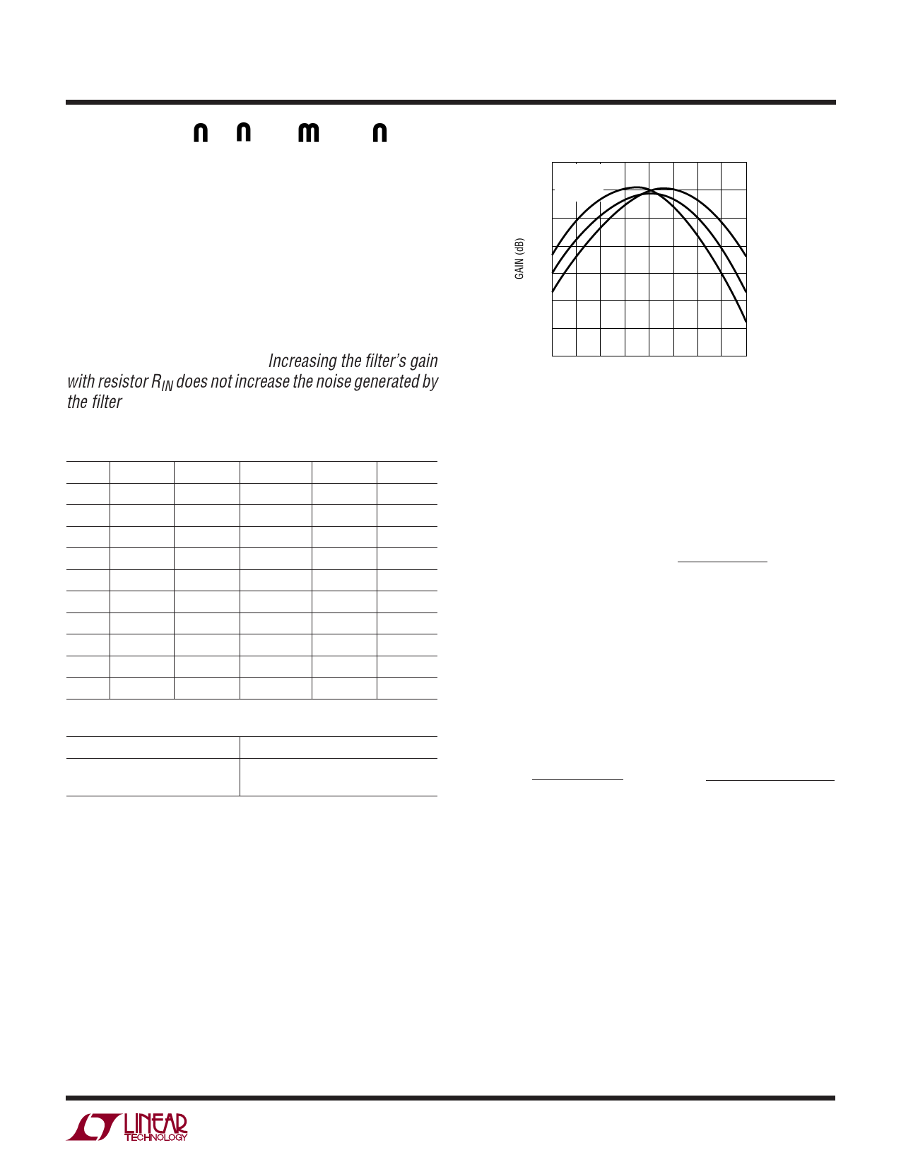
The passband of the LTC1164-8 is from 0.995 • fCENTER to
1.005 • fCENTER. At the passband’s end points the typical
filter gain is – 3dB ±2dB relative to the gain at fCENTER.
Figure 3 shows typical passband gain variations versus
percent of frequency deviation from fCENTER. Outside the
filter’s passband, signal attenuation increases to – 50dB
for frequencies less than 0.96 • fCENTER and greater than
1.04 • fCENTER.
In applications where a signal is to be detected in the
presence of wideband noise, the ultraselectivity of the
LTC1164-8 can improve the output signal-to-noise ratio.
When wideband noise (white noise) appears at the input to
3
VS = ±5V
0
RIN = 340k
RF = 61.9k
–3
–6
–9
–12
–15
–18
–1.00
–0.50 fCENTER 0.50
1.00
PERCENT DEVIATION FROM fCENTER (±% fCENTER)
LTC1164-8 • F03
Figure 3. Typical Passband Variations
the filter, only a small amount of input noise will reach the
filter’s output. If the output noise of the LTC1164-8 is
neglected, the signal-to-noise ratio at the output of the
filter divided by the signal-to-noise ratio at the input of the
filter equals:
(S/N)OUT/(S/N)IN = 20 • Log √(BW)IN/(BW)f
where,
(BW)IN = noise bandwidth at the input of the filter
(BW)f = 0.01 • fCENTER = noise equivalent filter bandwidth
Example: A small 1kHz signal is sent through a cable that
also conducts random noise. The cable bandwidth is
3.4kHz. An LTC1164-8 is used to detect the 1kHz signal.
The signal-to-noise ratio at the output of the filter is 25.3dB
larger than the signal-to-noise ratio at the input of the filter
(20 • Log√(BW)IN/(BW)f = 20 • Log√3.4kHz/ 0.01 • 1kHz
1kHz = 25.3dB).
The AC output swing with ±5V supplies is ±4V, with a
single 5V supply it is 1V to 4V, when AGND (Pins 3, 5) is
biased at 2.5V. Table 4 lists op amps that are recom-
mended for use with an LTC1164-8. The LTC1164-8 is
designed and specified for a dual ±5V or single 5V supply
operation. The filter’s passband gain linearity is optimum
at single 5V supply and with Pins 3, 5 (AGND) biased at 2V.
Filter operation at ±7.5V supplies is not tested or speci-
fied. At VS = 7.5V, the filter will operate with center
frequencies up to 7kHz. Please refer to the Passband
Variations vs Power Supply graph in the Typical Perfor-
mance Characteristics.
7
Share Link: