LTC1164-8(RevA) 查看數據表(PDF) - Linear Technology
零件编号
产品描述 (功能)
生产厂家
LTC1164-8
(Rev.:RevA)
(Rev.:RevA)
Linear Technology

LTC1164-8 Datasheet PDF : 12 Pages
| |||
LTC1164-8
APPLICATIONS INFORMATION
Printed Circuit Layout
For optimum filter performance, an LTC1164-8 should be
operating on a printed circuit board that has been laid out
for precision analog signal processing circuits. On a
printed circuit board, an LTC1164-8 should be surrounded
with an adequate analog signal ground plane and its power
supply pins bypassed to ground with 0.1µF capacitors.
The ground plane of an LTC1164-8 and any digital ground
plane should preferably meet at a single point on a system
ground (star system ground).
The following external filter connections should be one
inch or less:
N Package
Resistor RIN to Pin 2
Pin 14 to Pin 7
Pin 9 to the Inverting Node of an External Op Amp
Ground Pins 1, 3, 5, 6, 8, 10 and 13
SW Package
Resistor RIN to Pin 2
Pin 16 to Pin 8
Pin 9 to the Inverting Node of External Op Amp
Ground Pins 1, 3, 5, 6, 7, 10, 11, 13 and 15
Any signal or power supply printed circuit traces should
be at least 0.2 inches away from the above mentioned
connections (this rule applies also to the routing of the
printed circuit trace originating from a clock source in a
digital circuit and terminating at a clock input pin of an
LTC1164-8). Operating an LTC1164-8 in an IC socket is
not recommended.
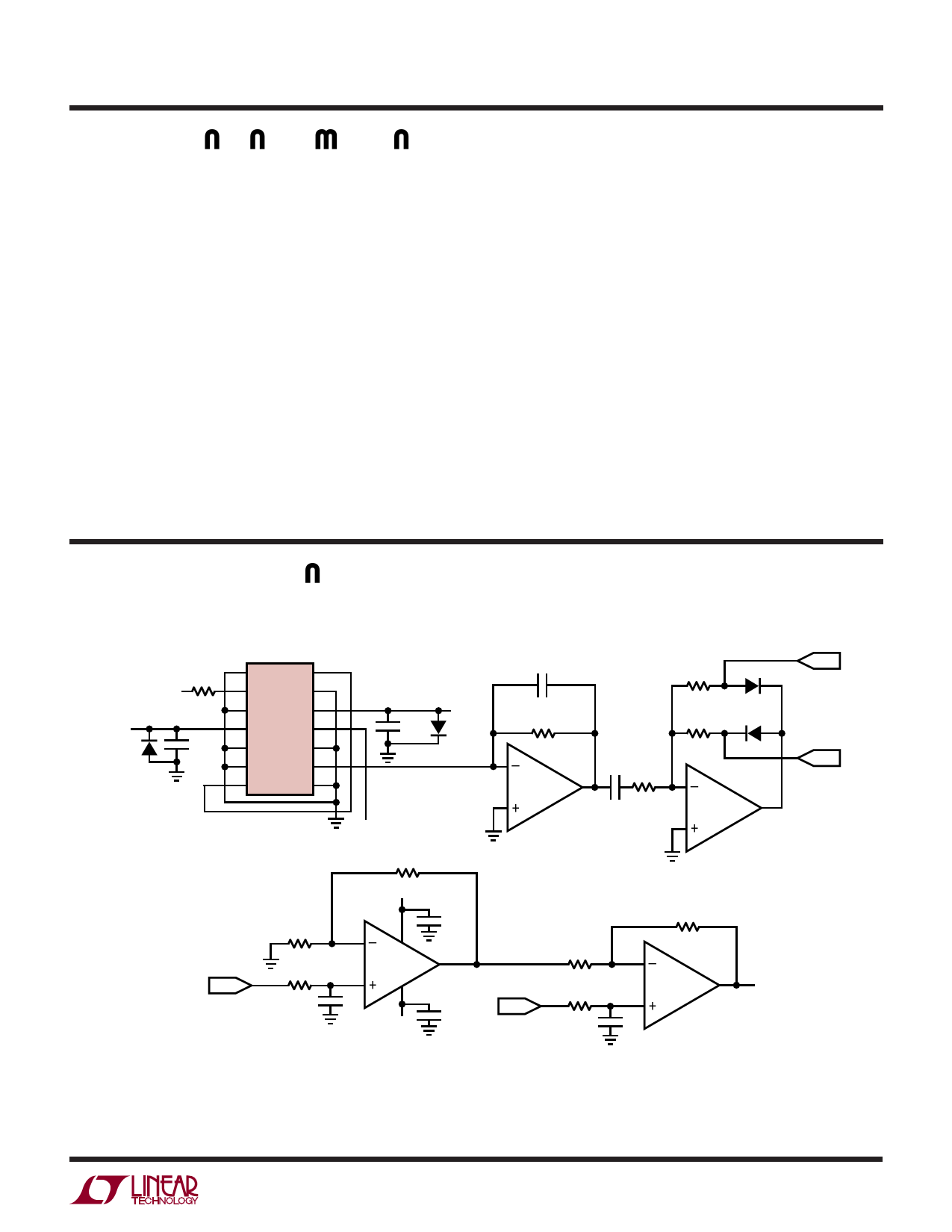
TYPICAL APPLICATIONS N
Tone Detector and Average Value Circuit
5V
1N4148
RIN
340k
VIN
1
14
2
13
3
12
4 LTC1164-8 11
0.1µF
– 5V
1N4148
CF
RF
61.9k
A
5k
1N458
5k
1N458
0.1µF 5
6
7
10
9
8
fCLK
100kHz
–
C1 R1
B
10k
–
1/2 LT1413
+
1/2 LT1413
+
5k
5V
0.1µF
5k
–4
5k
R2
1/2 LT1413
100k
+
A
11
C2
R3
100k
B
0.1µF
– 5V
VOUT = AVERAGE OF ABS [VPEAK × SIN (2π × fCENTER × t)], ±10% FROM 1VP-P TO 7VP-P
RIN = 340k/GAIN; fCENTER = fCLK/100; 1/(2π × RF × CF) ≥ 10 × fCENTER
1/(2π × R1 × C1) ≤ fCENTER/10; 1/(2π × R2 × C2) ≤ fCENTER/25; R2 × C2 = R3 × C3
5k
–
1/2 LT1413
+
C3
VOUT
LTC1164-8 • TA03
9
Share Link: