LTC1164-6(Rev0) 查看數據表(PDF) - Linear Technology
零件编号
产品描述 (功能)
生产厂家
LTC1164-6
(Rev.:Rev0)
(Rev.:Rev0)
Linear Technology

LTC1164-6 Datasheet PDF : 12 Pages
| |||
LTC1164-6
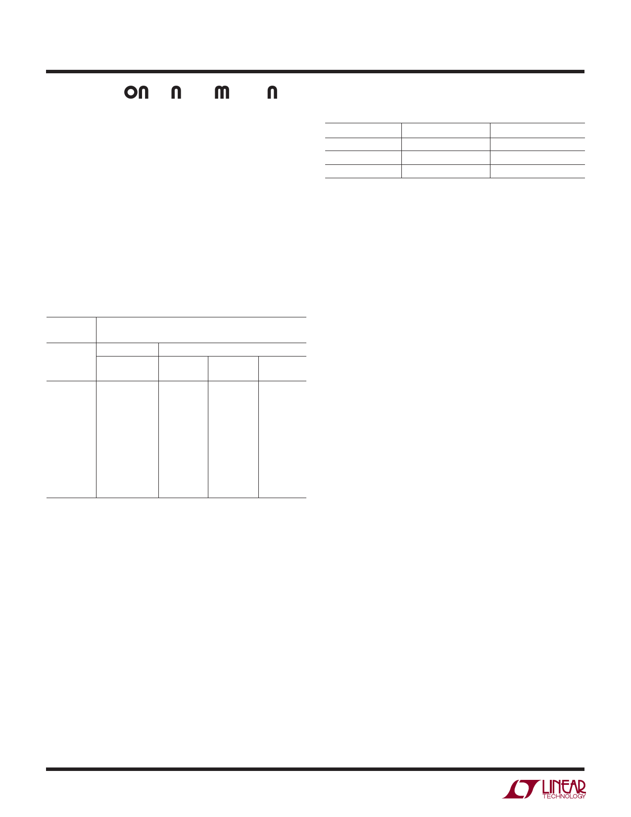
PI FU CTIO S (14-Lead Dual-In-Line Package)
can be used provided that its input common-mode range
is well within the filter’s output swing. Pin 6 is an interme-
diate filter output providing an unspecified 6th order
lowpass filter. Pin 6 should not be loaded.
–
1k
+
LT1006, fC < 5kHz
LT1200, fC > 5kHz
1164-6 F03
Figure 3. Buffer for Filter Output
External Connection Pins (7, 14)
Pins 7 and 14 should be connected together. In a printed
circuit board the connection should be done under the IC
package through a short trace surrounded by the analog
ground plane.
NC Pin (1, 8, 13)
Pins 1, 8, and 13 are not connected to any internal circuit
point on the device and should preferably be tied to analog
ground.
APPLICATI S I FOR ATIO
Passband Response
The passband response of the LTC1164-6 is optimized for
a fCLK/fCUTOFF ratio of 100:1. Minimum passband ripple
occurs from 1Hz to 80% of fCUTOFF. Athough the passband
of the LTC1164-6 is optimized for ratio fCLK / fCUTOFF of
100:1, if a ratio of 50:1 is desired, connect a single pole
lowpass RC (f –3dB = 2 fCUTOFF) at the output of the filter.
The RC will make the passband gain response as flat as the
100:1 case. If the RC is omitted, and clock frequencies are
below 500kHz the passband gain will peak by 0.4dB at
90% fCUTOFF.
Table 2. Typical Passband Ripple with Single 5V Supply
(fCLK/fC) = 100:1, GND = 2V, 30kHz, Fixed Single Pole, Lowpass
RC Filter at Pin 9 (See Typical Applications)
PASSBAND
FREQUENCY
% of fCUTOFF
10
20
30
40
50
60
70
80
90
fCUTOFF
PASSBAND GAIN
(REFERENCED TO 0dB)
fCUTOFF = 1kHz
TA = 25°C
(dB)
fCUTOFF = 10kHz
TA = 0°C TA = 25°C TA = 70°C
(dB)
(dB)
(dB)
0.00
– 0.02
– 0.05
– 0.10
– 0.13
– 0.15
– 0.18
– 0.25
– 0.39
– 2.68
0.00
0.00
– 0.01
– 0.02
– 0.03
– 0.01
– 0.01
– 0.08
– 0.23
– 2.79
0.00
0.01
– 0.01
– 0.02
– 0.01
0.01
0.01
– 0.05
– 0.18
– 2.74
0.00
0.01
0.01
0.02
0.03
0.05
0.07
0.02
– 0.05
– 2.68
The gain peaking can approximate a sin χ/χ correction for
some applications. (See Typical Performance Characteris-
tics curve, Passband vs Frequency and fCLK at fCLK / fC =
50:1.)
When the LTC1164-6 operates with a single 5V supply and
its cutoff frequency is clock-tuned to 10kHz, an output
single pole RC filter can also help maintain outstanding
passband flatness from 0°C to 70°C. Table 2 shows
details.
Clock Feedthrough
Clock feedthrough is defined as, the RMS value of the clock
frequency and its harmonics that are present at the filter’s
output pin (9). The clock feedthrough is tested with the
input pin (2) grounded and, it depends on PC board layout
and on the value of the power supplies. With proper layout
techniques the values of the clock feedthrough are shown
in Table 3.
Table 3. Clock Feedthrough
VS
±2.5V
±5V
±7.5V
50:1
60µVRMS
100µVRMS
150µVRMS
100:1
60µVRMS
200µVRMS
500µVRMS
Note: The clock feedthrough at ±2.5V supplies is imbedded in the wideband
noise of the filter. (The clock signal is a square wave.)
8
Share Link: