EN80C186EA25 查看數據表(PDF) - Intel
零件编号
产品描述 (功能)
生产厂家
EN80C186EA25 Datasheet PDF : 56 Pages
| |||
Intel® 80C186XL and Intel® 80C186EA Differences
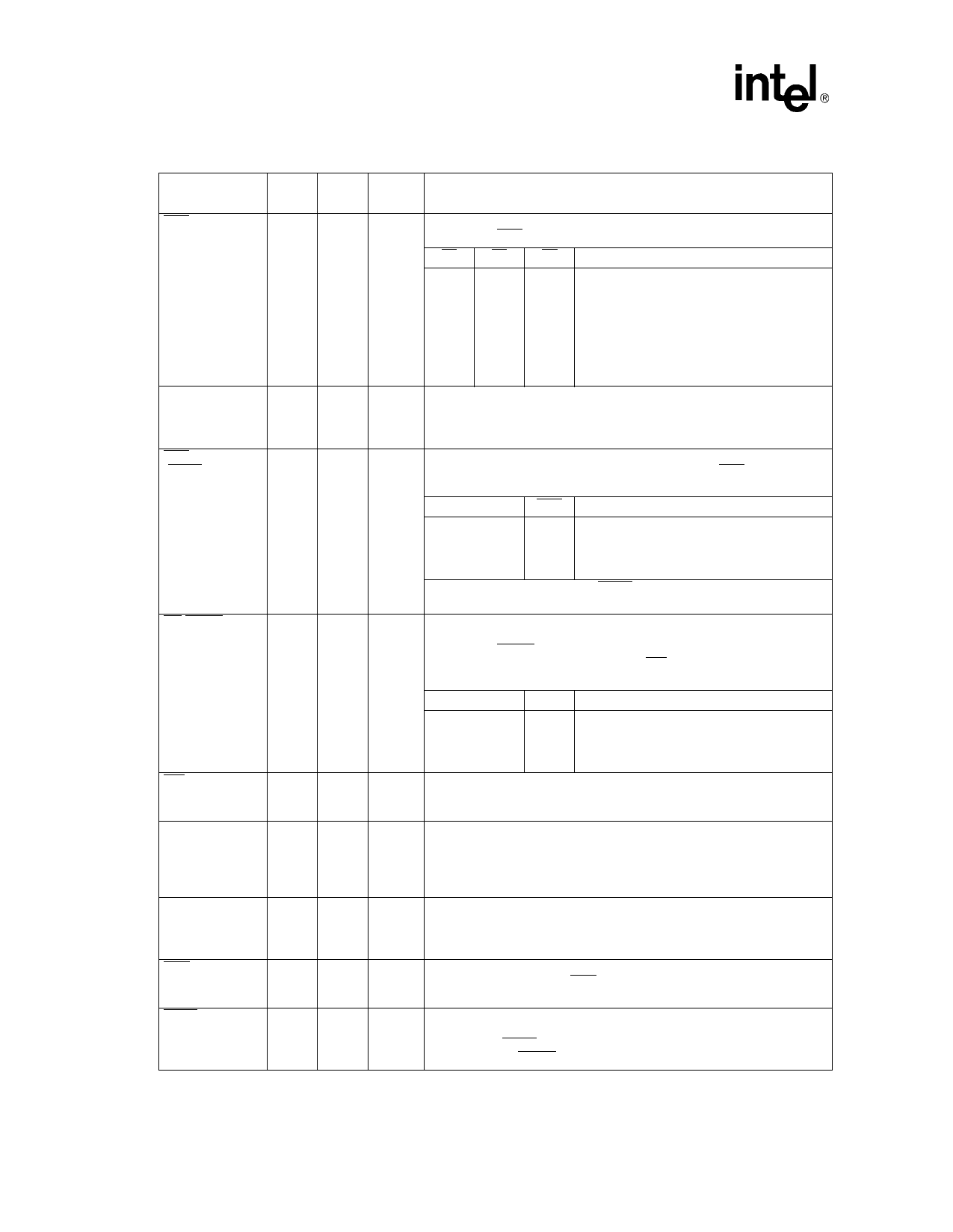
Table 5.
Pin Descriptions (Sheet 2 of 3)
Pin Name
S2:0
ALE/QS0
BHE
(RFSH)
RD/QSMD
WR/QS1
ARDY
SRDY
DEN
LOCK
Pin
Type
O
O
O
O
O
I
I
O
O
Input
Type
S(L)
H(Z)
R(Z)
P(1)
Output
States
Description
H(Z)
R(Z)
P(1)
Bus cycle Status are encoded on these pins to provide bus transaction
information. S2:0 are encoded as follows:
S2
S1
S0 Bus Cycle Initiated
0
0
0 Interrupt Acknowledge
0
0
1 Read I/O
0
1
0 Write I/O
0
1
1 Processor HALT
1
0
0 Queue Instruction Fetch
1
0
1 Read Memory
1
1
0 Write Memory
1
1
1 Passive (no bus activity)
H(0) Address Latch Enable output is used to strobe address information into
R(0) a transparent type latch during the address phase of the bus cycle. In
P(0) Queue Status Mode, QS0 provides queue status information along with
QS1.
H(Z)
R(Z)
P(X)
Byte High Enable output to indicate that the bus cycle in progress is
transferring data over the upper half of the data bus. BHE and A0 have
the following logical encoding:
A0
BHE Encoding (For 80C186EA/80L186EA Only)
0
0 Word Transfer
0
1 Even Byte Transfer
1
0 Odd Byte Transfer
1
1 Refresh Operation
On the 80C188EA/80L188EA, RFSH is asserted low to indicate a
Refresh bus cycle.
H(Z)
R(WH)
P(1)
ReaD output signals that the accessed memory or I/O device must drive
data information onto the data bus. Upon reset, this pin has an alternate
function. As QSMD, it enables Queue Status Mode when grounded. In
Queue Status Mode, the ALE/QS0 and WR/QS1 pins provide the
following information about processor/instruction queue interaction:
QS1
QS0 Queue Operation
0
0 No Queue Operation
0
1 First Opcode Byte Fetched from the Queue
1
1 Subsequent Byte Fetched from the Queue
1
0 Empty the Queue
H(Z)
R(Z)
P(1)
WRite output signals that data available on the data bus are to be written
into the accessed memory or I/O device. In Queue Status Mode, QS1
provides queue status information along with QS0.
A(L) Asynchronous ReaDY is an input to signal for the end of a bus cycle.
S(L) ARDY is asynchronous on rising CLKOUT and synchronous on falling
CLKOUT. ARDY or SRDY must be active to terminate any processor bus
cycle, unless they are ignored due to correct programming of the Chip
Select Unit.
Synchronous ReaDY is an input to signal for the end of a bus cycle.
ARDY or SRDY must be active to terminate any processor bus cycle,
unless they are ignored due to correct programming of the Chip Select
Unit.
Data ENable output to control the enable of bidirectional transceivers
when buffering a system. DEN is active only when data is to be
transferred on the bus.
H(Z)
R(WH)
P(1)
LOCK output indicates that the bus cycle in progress is not to be
interrupted. The processor will not service other bus requests (such as
HOLD) while LOCK is active. This pin is configured as a weakly held
high input while RESIN is active and must not be driven low.
20
Product Name Datasheet
Share Link: 