AD7249(2000) 查看數據表(PDF) - Analog Devices
零件编号
产品描述 (功能)
生产厂家
AD7249 Datasheet PDF : 12 Pages
| |||
AD7249
SCLK
SYNC
SDIN
LDAC
CLR
t1
t2
t5
t4
DB15 DB14 DB13 DB12 DB11
DON'T DON'T DON'T DAC MSB
CARE CARE CARE SELECT
=0
DAC A
t3
t10
DB0
LSB
DB15 DB14 DB13 DB12 DB10
DON'T DON'T DON'T DAC MSB
CARE CARE CARE SELECT
=1
DAC B
DB0
LSB
t6
t7
t8
t9
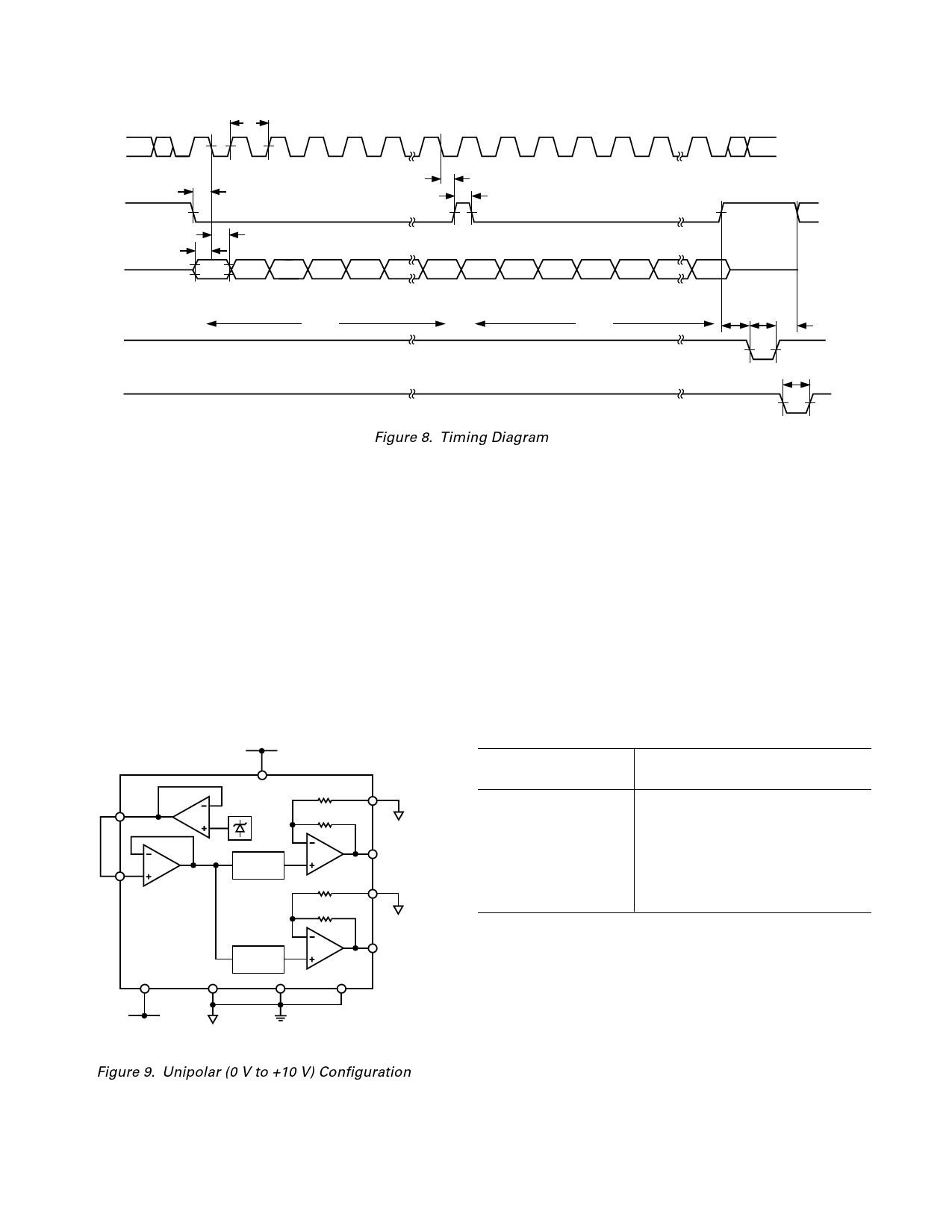
Figure 8. Timing Diagram
TRANSFER FUNCTION
The internal scaling resistors provided on the AD7249 allow
several output voltage ranges. The part can produce unipolar
output ranges of 0 V to +5 V or 0 V to +10 V and a bipolar
output range of ± 5 V. Connections for the various ranges are
outlined below. Since each DAC has its own ROFS input the two
DACs can be set up for different output ranges.
Unipolar (0 V to +10 V) Configuration
The first of the configurations provides an output voltage range
of 0 V to +10 V. This is achieved by connecting the output
offset resistor ROFSA, ROFSB (Pin 3, 16) to AGND. Natural Bi-
nary data format is selected by connecting BIN/COMP (Pin 7)
to DGND. In this configuration, the AD7249 can be operated
using either single or dual supplies. Note that the VDD supply is
REFOUT
VDD
VDD
2R
2R
ROFSA
REFIN
A1
12-BIT
DAC A
2R
2R
VOUTA
0V TO 10V
ROFSB
AD7249*
A2
12-BIT
DAC B
VOUTB
0V TO 10V
VSS
0V OR VSS
AGND
DGND
BIN/COMP
*ADDITIONAL PINS OMITTED FOR CLARITY.
Figure 9. Unipolar (0 V to +10 V) Configuration
restricted to +15 V ± 10% for this range in order to maintain
sufficient amplifier headroom. Dual supplies may be used to
improve settling time and give increased current sink capability
for the amplifier. Figure 9 shows the connection diagram for
unipolar operation of the AD7249. Table I shows the digital
code vs. analog output for this configuration.
Unipolar (0 V to +5 V) Configuration
The 0 V to +5 V output voltage range is achieved by tying
ROFSA to VOUTA or ROFSB to VOUTB. Once again, the AD7249
can be operated using either single or dual supplies. The table
for output voltage versus digital code is as in Table I, with
2REFIN replaced by REFIN. Note, for this range, 1 LSB =
REFIN × (2–12) = (REFIN/4096).
Table I. Unipolar Code Table (0 V to +10 V Range)
Input Data Word
MSB LSB
XXXY 1111 1111 1111
XXXY 1000 0000 0001
XXXY 1000 0000 0000
XXXY 0111 1111 1111
XXXY 0000 0000 0001
XXXY 0000 0000 0000
Analog Output, VOUT
+2REFIN × (4095/4096)
+2REFIN × (2049/4096)
+2REFIN × (2048/4096) = +REFIN
+2REFIN × (2047/4096)
+2REFIN × (1/4096)
0V
X = Don’t Care.
Y = DAC Select Bit, 0 = DAC A, 1= DAC B.
Note: 1 LSB = 2REFIN/4096.
–8–
REV. C
Share Link: 