FDB5690 查看數據表(PDF) - Fairchild Semiconductor
零件编号
产品描述 (功能)
生产厂家
FDB5690 Datasheet PDF : 16 Pages
| |||
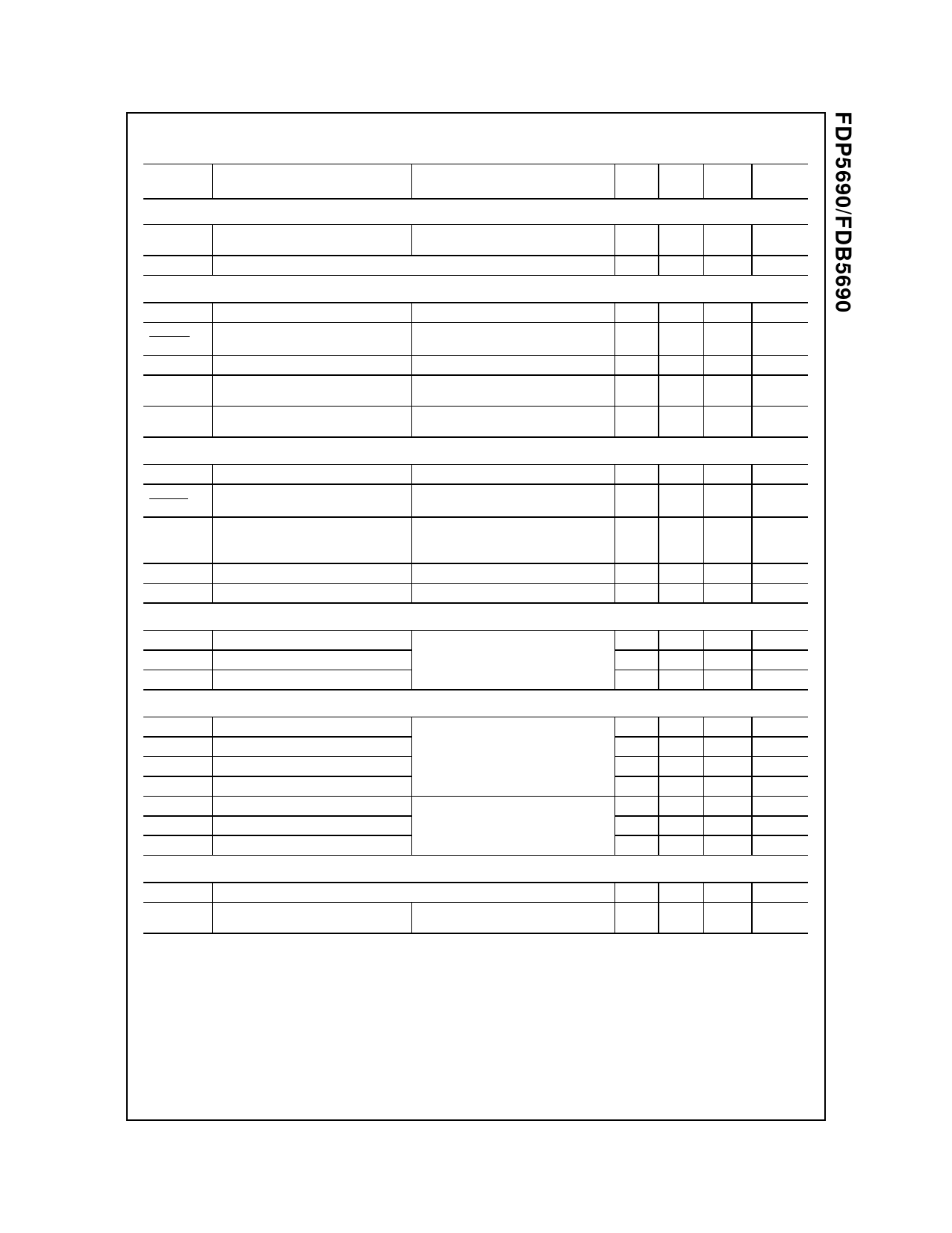
Electrical Characteristics
Symbol
Parameter
Tc = 25°C unless otherwise noted
Test Conditions
Min Typ Max Units
Drain-Source Avalanche Ratings (Note1)
WDSS
Single Pulse Drain-Source
Avalanche Energy
VDD = 30 V, ID = 32A
IAR
Maximum Drain-Source Avalanche Current
80
mJ
32
A
Off Characteristics
BVDSS
Drain-Source Breakdown Voltage VGS = 0 V, ID = 250 µA
60
V
∆BVDSS Breakdown Voltage Temperature ID = 250 µA, Referenced to 25°C
61
mV/°C
∆TJ
Coefficient
IDSS
Zero Gate Voltage Drain Current VDS = 48 V, VGS = 0 V
1
µA
IGSSF
Gate-Body Leakage Current,
Forward
VGS = 20 V, VDS = 0 V
100
nA
IGSSR
Gate-Body Leakage Current,
Reverse
VGS = -20 V, VDS = 0 V
-100
nA
On Characteristics (Note 1)
VGS(th)
Gate Threshold Voltage
∆VGS(th)
∆TJ
RDS(on)
Gate Threshold Voltage
Temperature Coefficient
Static Drain-Source
On-Resistance
ID(on)
On-State Drain Current
gFS
Forward Transconductance
VDS = VGS, ID = 250 µA
ID = 250 µA, Referenced to 25°C
VGS = 10 V, ID = 16 A,
VGS = 10 V, ID = 16 A,TJ = 125°C
VGS = 6 V, ID = 15 A
VGS = 10 V, VDS = 5 V
VDS = 5 V, ID = 16 A
2
2.4
4
V
-6.4
mV/°C
0.021 0.027
Ω
0.042 0.055
0.024 0.032
50
A
32
S
Dynamic Characteristics
Ciss
Input Capacitance
Coss
Output Capacitance
Crss
Reverse Transfer Capacitance
VDS = 25 V, VGS = 0 V,
f = 1.0 MHz
1120
pF
160
pF
80
pF
Switching Characteristics
td(on)
Turn-On Delay Time
tr
Turn-On Rise Time
td(off)
Turn-Off Delay Time
tf
Turn-Off Fall Time
Qg
Total Gate Charge
Qgs
Gate-Source Charge
Qgd
Gate-Drain Charge
(Note 1)
VDD = 30 V, ID = 1 A,
VGS = 10 V, RGEN = 6 Ω
VDS = 15 V,
ID = 16 A, VGS = 10 V
10
18
ns
9
18
ns
24
39
ns
10
18
ns
23
33
nC
3.9
nC
6.8
nC
Drain-Source Diode Characteristics and Maximum Ratings
IS
Maximum Continuous Drain-Source Diode Forward Current (Note 1)
VSD
Drain-Source Diode Forward
Voltage
Note:
1. Pulse Test: Pulse Width ≤ 300 µs, Duty Cycle ≤ 2.0%
VGS = 0 V, IS = 16 A
(Note 1)
32
A
0.92 1.2
V
FDP5690/FDB5690 Rev. C
Share Link: 