HI5735 查看數據表(PDF) - Renesas Electronics
零件编号
产品描述 (功能)
生产厂家
HI5735 Datasheet PDF : 11 Pages
| |||
HI5735
Pin Descriptions
PIN NUMBER PIN NAME
PIN DESCRIPTION
1-12
D11 (MSB) thru Digital Data Bit 11, the Most Significant Bit thru Digital Data Bit 0, the Least Significant Bit.
D0 (LSB)
15
CLK
Data Clock Pin DC to 80 MSPS.
13, 14
NC
No Connect.
16
17, 28
VCC
DGND
Digital Logic Supply +5V.
Digital Ground.
18
DVEE
-5.2V Logic Supply.
23
RSET
External resistor to set the full scale output current. IFS = 16 x (VREF OUT / RSET). Typically 976.
27
AGND
Analog Ground supply current return pin.
19
ARTN
Analog Signal Return for the R/2R ladder.
21
IOUT
Current Output Pin.
20
IOUT
Complementary Current Output Pin.
22
AVEE
-5.2V Analog Supply.
24
CTRL IN Input to the current source base rail. Typically connected to CTRL OUT and a 0.1F capacitor to AVEE. Allows
external control of the current sources.
25
CTRL OUT Control Amplifier Out. Provides precision control of the current sources when connected to CTRL IN such that
IFS = 16 x (VREF OUT / RSET).
26
REF OUT -1.23V (typical) bandgap reference voltage output. Can sink up to 125A or be overdriven by an external
reference capable of delivering up to 2mA.
Detailed Description
The HI5735 is a 12-bit, current out D/A converter. The DAC can
convert at 80 MSPS and runs on +5V and -5.2V supplies. The
architecture is an R/2R and segmented switching current cell
arrangement to reduce glitch. Laser trimming is employed to
tune linearity to true 12-bit levels. The HI5735 achieves its low
power and high speed performance from an advanced BiCMOS
process. The HI5735 consumes 650mW (typical) and has an
improved hold time of only 0.25ns (typical).
Digital Inputs
The HI5735 is a TTL/CMOS compatible D/A. Data is latched by
a Master register. Once latched, data inputs D0 (LSB) thru D11
(MSB) are internally translated from TTL to ECL. The internal
latch and switching current source controls are implemented in
ECL technology to maintain high switching speeds and low
noise characteristics.
Decoder/Driver
The architecture employs a split R/2R ladder and Segmented
Current source arrangement. Bits D0 (LSB) thru D7 directly
drive a typical R/2R network to create the binary weighted
current sources. Bits D8 thru D11 (MSB) pass thru a
“thermometer” decoder that converts the incoming data into 15
individual segmented current source enables. This split
architecture helps to improve glitch, thus resulting in a more
constant glitch characteristic across the entire output transfer
function.
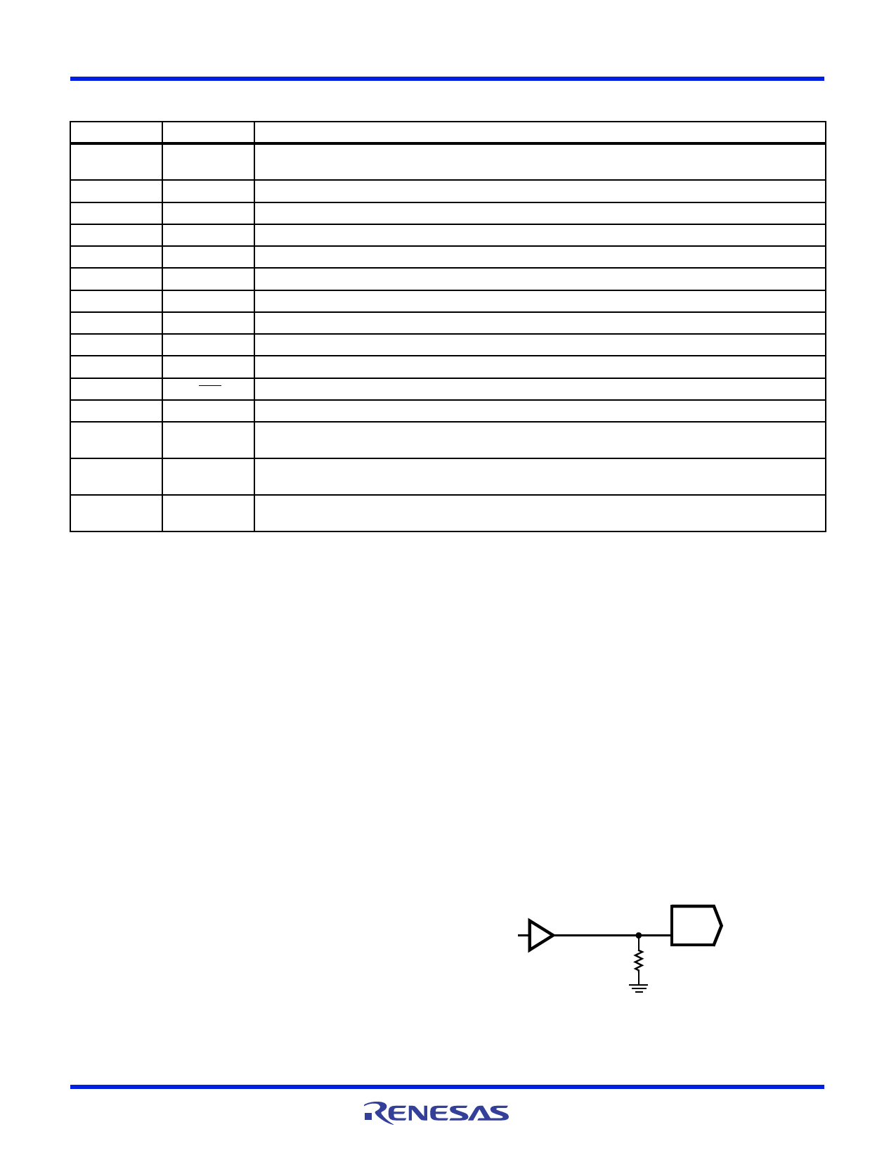
Clocks and Termination
The internal 12-bit register is updated on the rising edge of the
clock. Since the HI5735 clock rate can run to 80 MSPS, to
minimize reflections and clock noise into the part, proper
termination should be used. In PCB layout clock runs should
be kept short and have a minimum of loads. To guarantee
consistent results from board to board, controlled impedance
PCBs should be used with a characteristic line impedance ZO
of 50.
To terminate the clock line, a shunt terminator to ground is the
most effective type at a 80 MSPS clock rate. A typical value for
termination can be determined by the equation:
RT = ZO,
for the termination resistor. For a controlled impedance board
with a ZO of 50, the RT = 50. Shunt termination is best
used at the receiving end of the transmission line or as close to
the HI5735 CLK pin as possible.
ZO = 50
CLK
HI5735
DAC
RT = 50
FIGURE 10. CLOCK LINE TERMINATION
FN4133 Rev 4.00
May 2003
Page 7 of 11
Share Link: 