LC7871E 查看數據表(PDF) - SANYO -> Panasonic
零件编号
产品描述 (功能)
生产厂家
LC7871E Datasheet PDF : 19 Pages
| |||
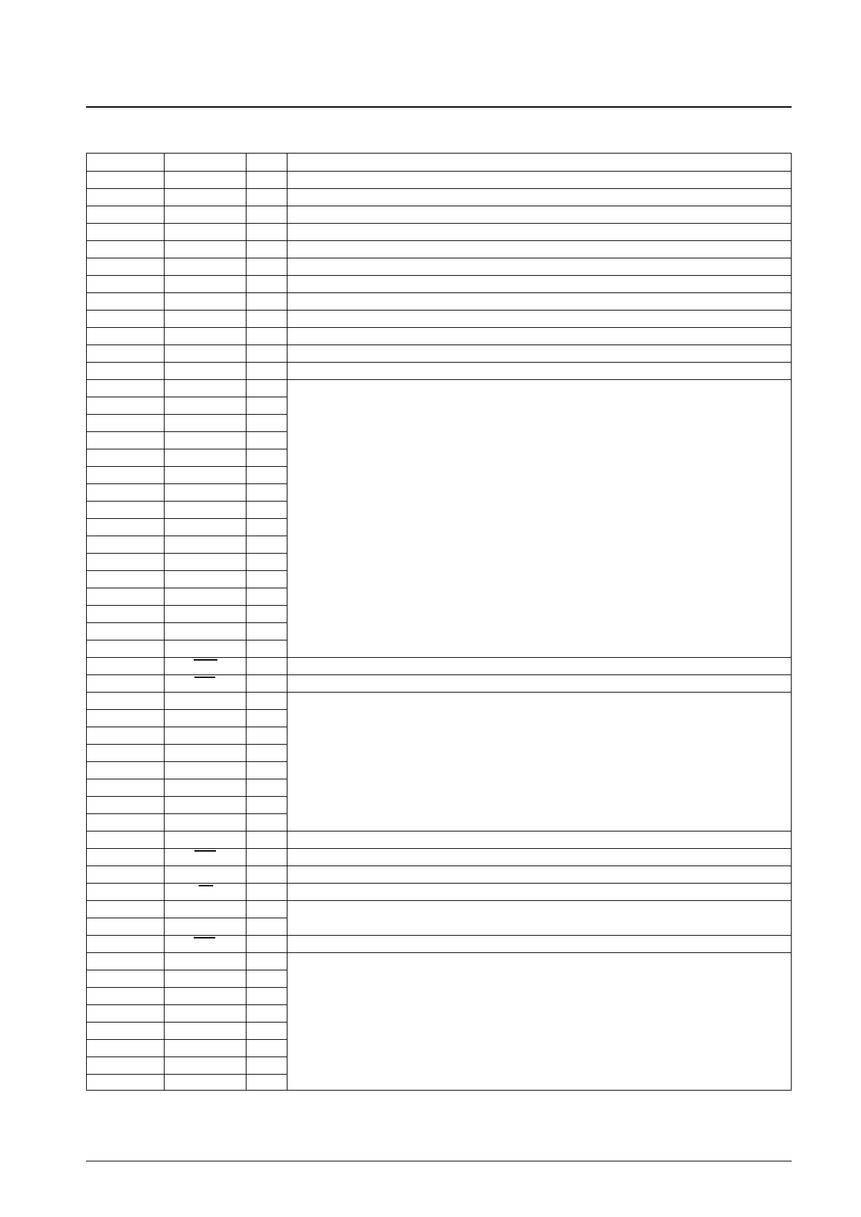
Pin Functions
Pin No.
1
2
3
4
5
6
7
8
9
10
11
12
13
14
15
16
17
18
19
20
21
22
23
24
25
26
27
28
29
30
31
32
33
34
35
36
37
38
39
40
41
42
43
44
45
46
47
48
49
50
51
52
53
Pin
S
SBCK
SFSY
PW
SBSY
VDD1
CE
DO
DI
CL
MUTE
VSS1
CH0
CH1
CH2
CH3
CH4
CH5
CH6
CH7
CH8
CH9
CH10
CH11
CH12
CH13
CH14
CH15
1WE
RAS
1A0
1A1
1A2
1A3
1A4
1A5
1A6
1A7
1DB0
CAS
1DB1
OE
1DB2
1DB3
2WE
2A0
2A1
2A2
2A3
2A4
2A5
2A6
2A7
LC7871E, 7871NE
I/O
Function
I CD DSP selection: High level input: LC7861N/67, middle level input: LC7860K/63, low level input: LC7868/69
O P to W subcode read clock
I Subcode frame synchronization signal
I P to W subcode data
I Subcode block synchronization signal
— Digital system power supply
I Control during serial input or serial output
O Serial data output
I Serial data input
I Serial data I/O clock
I Control signal used to specify that the subcode data be handled as invalid
— Digital system ground
I
I
I
I
I
I
I
I Channel selection pins. A high level enables the corresponding channel.
I These pins have built-in pull-down resistors.
I
I
I
I
I
I
I
O Primary DRAM control
O Control pin shared by primary and secondary DRAM
O
O
O
O
Primary DRAM address
O
O
O
O
I/O Primary DRAM data
O Control pin shared by primary and secondary DRAM
I/O Primary DRAM data
O Control pin shared by primary and secondary DRAM
I/O
Primary DRAM data
I/O
O Secondary DRAM control
O
O
O
O
Secondary DRAM address
O
O
O
O
Continued on next page.
No. 4861-9/19
Share Link: 