MAX791M(1995) 查看數據表(PDF) - Maxim Integrated
零件编号
产品描述 (功能)
生产厂家
MAX791M Datasheet PDF : 20 Pages
| |||
Microprocessor Supervisory Circuit
VCC
RESET
THRESHOLD
CE IN
CE OUT
RESET
RESET
15µs
100µs
100µs
50Ω DRIVER
+5V
VCC
MAX791
CE IN
CE OUT
GND
CLOAD
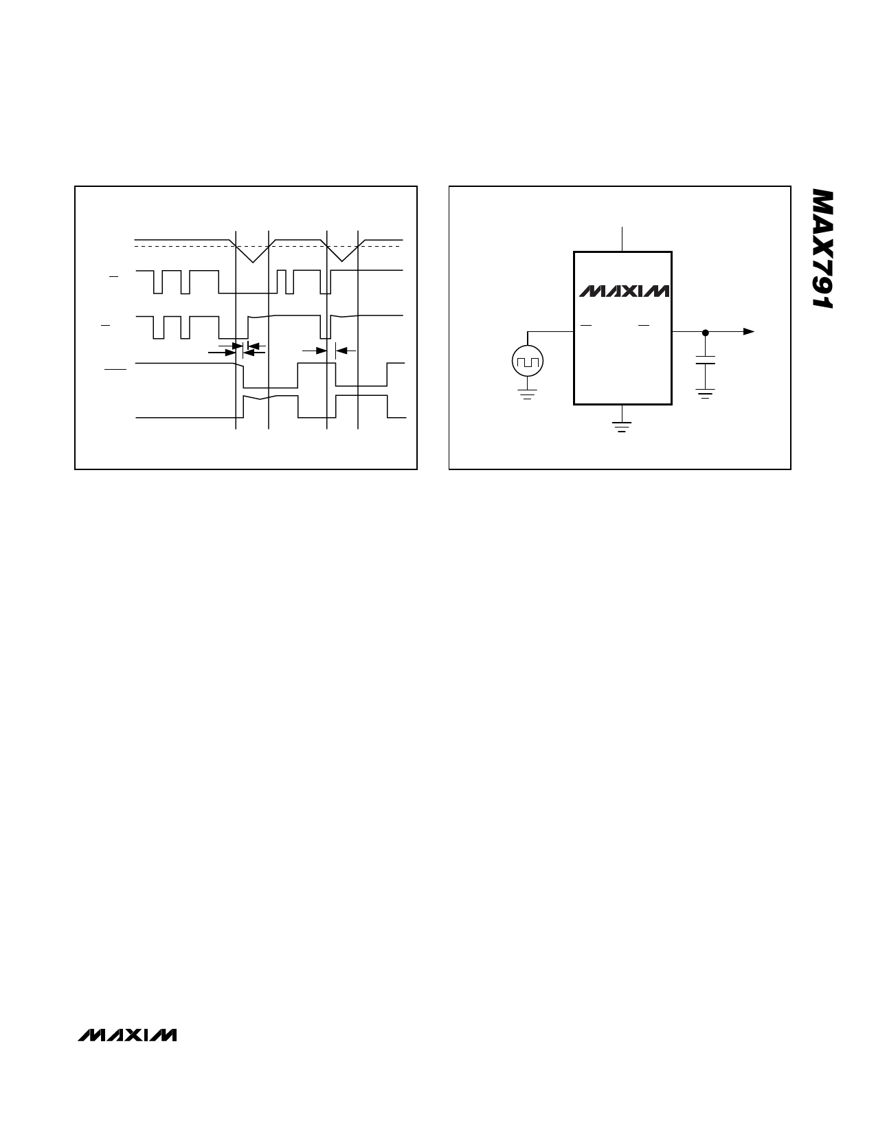
Figure 7. Reset and Chip-Enable Timing
Figure 8. CE Propagation Delay Test Circuit
Chip-Enable Signal Gating
The MAX791 provides internal gating of chip-enable
(CE) signals, to prevent erroneous data from corrupting
the CMOS RAM in the event of a power failure. During
normal operation, the CE gate is enabled and passes
all CE transitions. When reset is asserted, this path
becomes disabled, preventing erroneous data from
corrupting the CMOS RAM. The MAX791 uses a series
transmission gate from the Chip-Enable Input (CE IN) to
CE OUT (Figure 1).
The 10ns max CE propagation from CE IN to CE OUT
enables the MAX791 to be used with most µPs.
Chip-Enable Input
CE IN is high impedance (disabled mode) while RESET
is asserted.
During a power-down sequence were VCC passes
4.65V, CE IN assumes a high-impedance state when
the voltage at CE IN goes high or 15µs after reset is
asserted, whichever occurs first (Figure 7).
During a power-up sequence, CE IN remains high
impedance, regardless of CE IN activity, until reset is
deasserted following the reset-timeout period.
In the high-impedance mode, the leakage currents into
this input are ±1µA max over temperature. In the low-
impedance mode, the impedance of CE IN appears as
a 75Ω resistor in series with the load at CE OUT.
The propagation delay through the CE transmission
gate depends on both the source impedance of the
drive to CE IN and the capacitive loading on CE OUT
(see the Chip-Enable Propagation Delay vs. CE OUT
Load Capacitance graph in the Typical Operating
Characteristics). The CE propagation delay is produc-
tion tested from the 50% point on CE IN to the 50%
point on CE OUT using a 50Ω driver and 50pF of load
capacitance (Figure 8). For minimum propagation
delay, minimize the capacitive load at CE OUT and use
a low output-impedance driver.
Chip-Enable Output
In the enabled mode, the impedance of CE OUT is
equivalent to 75Ω in series with the source driving CE
IN. In the disabled mode, the 75Ω transmission gate is
off and CE OUT is actively pulled to VOUT. This source
turns off when the transmission gate is enabled.
LOWLINE Output
The low-line comparator monitors VCC with a typical
threshold voltage 150mV above the reset threshold,
and has 15mV of hysteresis. LOWLINE typically sinks
3.2mA at 0.1V. For normal operation (VCC above the
LOWLINE threshold), LOWLINE is pulled to VOUT. If
access to the unregulated supply is unavailable, use
LOWLINE to provide a nonmaskable interrupt (NMI) to
the µP as VCC begins to fall (Figure 9a).
______________________________________________________________________________________ 11
Share Link: 