SI3586DV-T1-E3 查看數據表(PDF) - VBsemi Electronics Co.,Ltd
零件编号
产品描述 (功能)
生产厂家
SI3586DV-T1-E3 Datasheet PDF : 10 Pages
| |||
SI3586DV-T1-E3
www.VBsemi.tw
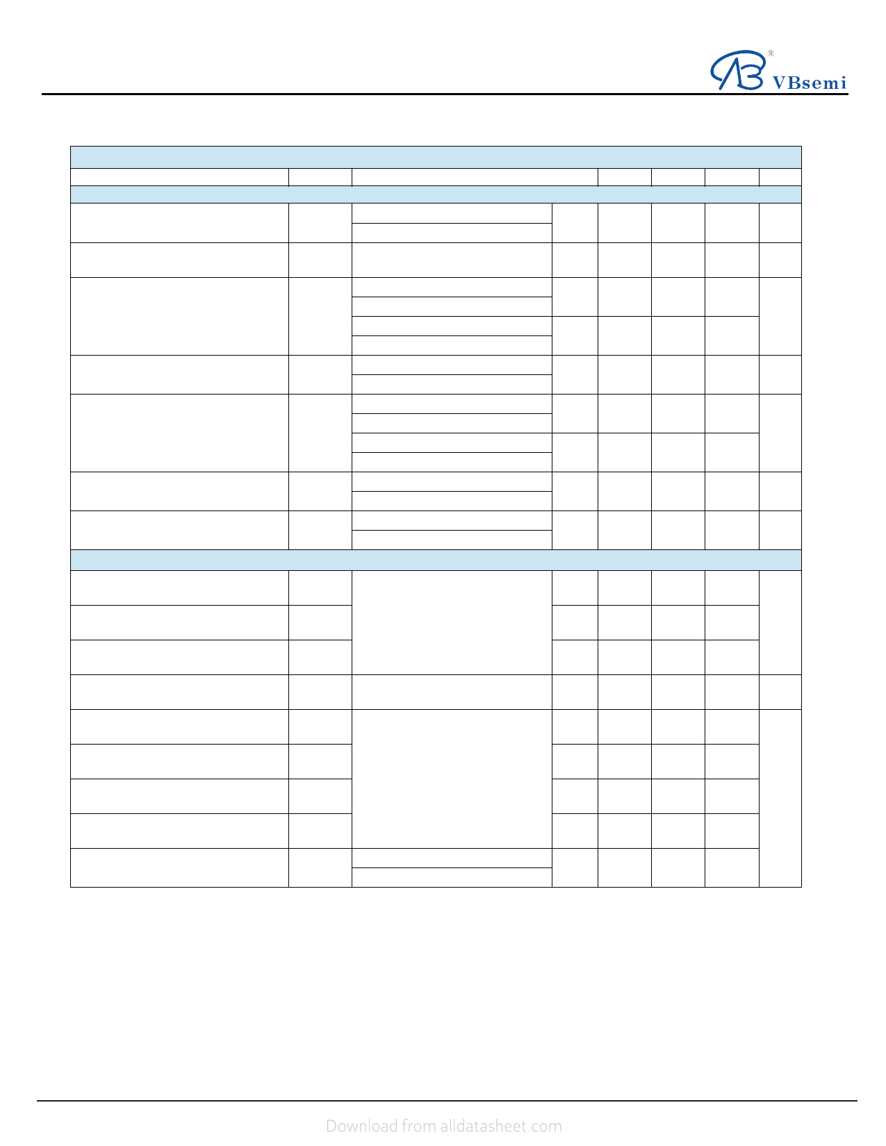
SPECIFICATIONS TJ = 25 °C, unless otherwise noted
Parameter
Symbol
Test Conditions
Static
Gate Threshold Voltage
VGS(th)
VDS = VGS, ID = 250 µA
VDS = VGS, ID = - 250 µA
Gate-Body Leakage
IGSS
VDS = 0 V, VGS = ± 20 V
Zero Gate Voltage Drain Current
On-State Drain Currenta
Drain-Source On-State Resistancea
Forward Transconductancea
Diode Forward Voltagea
Dynamicb
IDSS
ID(on)
RDS(on)
gfs
VSD
VDS = 24 V, VGS = 0 V
VDS = - 24 V, VGS = 0 V
VDS = 24 V, VGS = 0 V, TJ = 55 °C
VDS = - 24 V, VGS = 0 V, TJ = 55 °C
VDS = 5 V, VGS = 10 V
VDS = - 5 V, VGS = - 10 V
VGS = 10 V, ID = 2.5 A
VGS = - 10 V, ID = - 1.8 A
VGS = 4.5 V, ID = 2.0 A
VGS = - 4.5 V, ID = - 1.2 A
VDS = 10 V, ID = 2.5 A
VDS = - 15 V, ID = - 1.8 A
IS = 1.05 A, VGS = 0 V
IS = - 1.05 A, VGS = 0 V
Total Gate Charge
Gate-Source Charge
Gate-Drain Charge
Qg
N-Channel
VDS = 15 V, VGS = 5 V, ID = 1.8 A
Qgs
P-Channel
Qgd
VDS = - 15 V, VGS = - 5 V, ID = - 1.8 A
Gate Resistance
Rg
Turn-On Delay Time
Rise Time
td(on)
tr
N-Channel
VDD = 15 V, RL = 15 Ω
ID ≅ 1 A, VGEN = 10 V, Rg = 6 Ω
Turn-Off Delay Time
Fall Time
td(off)
tf
P-Channel
VDD = - 15 V, RL = 15 Ω
ID ≅ - 1 A, VGEN = - 10 V, Rg = 6 Ω
Source-Drain Reverse Recovery Time
trr
IF = 1.05 A, dI/dt = 100 A/µs
IF = - 1.05 A, dI/dt = 100 A/µs
Notes:
a. Pulse test; pulse width ≤ 300 µs, duty cycle ≤ 2 %.
b. Guaranteed by design, not subject to production testing.
N-Ch
P-Ch
N-Ch
P-Ch
N-Ch
P-Ch
N-Ch
P-Ch
N-Ch
P-Ch
N-Ch
P-Ch
N-Ch
P-Ch
N-Ch
P-Ch
N-Ch
P-Ch
N-Ch
P-Ch
N-Ch
P-Ch
N-Ch
P-Ch
N-Ch
P-Ch
N-Ch
P-Ch
N-Ch
P-Ch
N-Ch
P-Ch
N-Ch
P-Ch
N-Ch
P-Ch
Min.
0.6
- 0.7
3.7
-3
0.5
3
Typ.
0.022
0.055
0.030
0.079
4.3
2.4
0.81
- 0.83
2.1
2.4
0.7
0.9
0.7
0.8
7
8
9
12
13
12
5
7
35
30
Max. Unit
V
± 100
nA
± 100
1
-1
µA
5
-5
A
0.024
0.069
Ω
0.036
0.083
S
1.10
V
- 1.10
3.2
3.6
nC
2.4
Ω
11
11
12
14
18
20
18
ns
8
11
60
60
Stresses beyond those listed under “Absolute Maximum Ratings” may cause permanent damage to the device. These are stress ratings only, and functional operation
of the device at these or any other conditions beyond those indicated in the operational sections of the specifications is not implied. Exposure to absolute maximum
rating conditions for extended periods may affect device reliability.
E-mail:China@VBsemi TEL:86-755-83251052
2
Share Link: 