LTC692(Rev0) 查看數據表(PDF) - Linear Technology
零件编号
产品描述 (功能)
生产厂家
LTC692 Datasheet PDF : 16 Pages
| |||
LTC692/LTC693
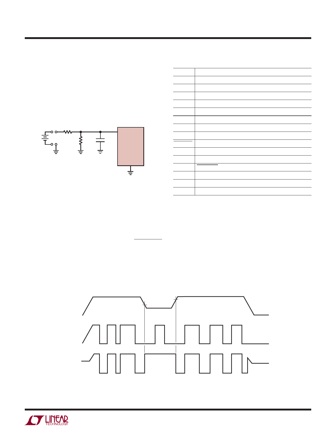
APPLICATI S I FOR ATIO
5V
0.1µF
3V
VCC
VOUT
LTC693
CE OUT
VBATT
GND
CE IN
RESET
RESET
+
10µF
0.1µF
VCC
62512
RAM
CSGND
20ns PROPAGATION DELAY
FROM DECODER
LTC692/3 • F06
TO µP
Figure 6. A Typical Nonvolatile CMOS RAM Application
5V
0.1µF
3V
VCC
VOUT
LTC692
VBATT RESET
GND
+
10µF
0.1µF
CS
VCC
62128
RAM
CS1
CS2
GND
LTC692/3 • F07
Figure 7. Write Protect for RAM with the LTC692
VIN ≥ 7.5V
+
10µF
R1
51k
R2
10k
LT1086-5
VIN VOUT
ADJ
+
100µF
R3
300k
5V
0.1µF
R4
10k
VCC
LTC692
LTC693
PFO
PFI GND
TO µP
LTC692/3 • F08
Figure 8. Monitoring Unregulated DC Supply with the
LTC692/LTC693 Power Fail Comparator
VIN ≥ 6.5V
+
10µF
LT1086-5
VIN VOUT
ADJ
+
10µF
5V
R1 R4
27k 10k
R3
2.7M
0.1µF
R2
8.2k
R5
3.3k
VCC
LTC692
LTC693
PFO
PFI GND
TO µP
LTC692/3 • F09
Figure 9. Monitoring Regulated DC Supply
with the LTC692/LTC693 Power Fail Comparator
Power Fail Warning
The LTC692/LTC693 generate a Power Failure Output
(PFO) for early warning of failure in the microprocessor's
power supply. This is accomplished by comparing the
Power Failure Input (PFI) with an internal 1.3V reference.
PFO goes low when the voltage at the PFI pin is less than
1.3V. Typically PFI is driven by an external voltage divider
(R1 and R2 in Figures 8 and 9) which senses either an
unregulated DC input or a regulated 5V output. The voltage
divider ratio can be chosen such that the voltage at the PFI
pin falls below 1.3V, several milliseconds before the 5V
supply falls below the maximum reset voltage threshold of
4.50V. PFO is normally used to interrupt the microproces-
sor to execute shutdown procedure between PFO and
RESET or RESET.
The power fail comparator, C3, does not have hysteresis.
Hysteresis can be added however, by connecting a resis-
tor between the PFO output and the noninverting PFI input
pin as shown in Figures 8 and 9. The upper and lower trip
points in the comparator are established as follows:
When PFO output is low, R3 sinks current from the
summing junction at the PFI pin.
VH
=
1.3V
1+
R1
R2
+
R1
R3
When PFO output is high, the series combination of R3 and
R4 source current into the PFI summing junction.
VL
=
1.3V
1 +
R1
R2
–
(5V – 1.3V)R1
1.3V(R3 + R4)
Assuming
R4 << R3,VHYSTERESIS
= 5V R1
R3
Example 1: The circuit in Figure 8 demonstrates the use of
the power fail comparator to monitor the unregulated
power supply input. Assuming the the rate of decay of the
supply input VIN is 100mV/ms and the total time to execute
a shutdown procedure is 8ms. Also, the noise of VIN is
200mV. With these assumptions in mind, we can reason-
ably set VL = 7.25V which is 1.25V greater than the sum of
maximum reset voltage threshold and the dropout voltage
of LT1086-5 (4.5V + 1.5V) and VHYSTERESIS = 850mV.
11
Share Link: 