MAX17435 查看數據表(PDF) - Maxim Integrated
零件编号
产品描述 (功能)
生产厂家
MAX17435 Datasheet PDF : 27 Pages
| |||
High-Frequency,
Low-Cost SMBus Chargers
The data (SDA) and clock (SCL) pins have Schmitt-
trigger inputs that can accommodate slow edges.
Choose pullup resistors for SDA and SCL to achieve rise
times according to the SMBus specifications.
Communication starts when the master signals a START
condition, which is a high-to-low transition on SDA, while
SCL is high. When the master has finished communicating,
the master issues a STOP condition, which is a low-to-
high transition on SDA, while SCL is high. The bus is
then free for another transmission. Figures 4 and 5 show
the timing diagrams for signals on the SMBus interface.
The address byte, command byte, and data bytes are
transmitted between the START and STOP conditions.
The SDA state is allowed to change only while SCL is
low, except for the START and STOP conditions. Data
is transmitted in 8-bit bytes and is sampled on the rising
edge of SCL. Nine clock cycles are required to transfer
each byte in or out of the MAX17435/MAX17535 because
either the master or the slave acknowledges the receipt
of the correct byte during the ninth clock. The MAX17435/
MAX17535 support the charger commands as described
in Table 4.
a) Write-Word Format
S
SLAVE
ADDRESS
W
ACK
COMMAND
BYTE
ACK
LOW DATA
BYTE
ACK
7 bits 1b 1b
8 bits
1b
8 bits
1b
MSB LSB 0 0
MSB LSB
0 MSB LSB 0
PRESET TO
0b0001001
Relearn() = 0x3D
D7
D0
ChargingCurrent() = 0x14
ChargerVoltage() = 0x15
HIGH DATA
BYTE
ACK P
8 bits
1b
MSB LSB 0
D15
D8
b) Read-Word Format
S
SLAVE
ADDRESS
W
ACK
COMMAND
BYTE
7 bits 1b 1b
8 bits
MSB LSB 0 0
MSB LSB
PRESET TO
0b0001001
INP_Voltage() = 0x3E
ACK S
SLAVE
ADDRESS
R ACK
LOW DATA
BYTE
ACK
HIGH DATA
BYTE
NACK P
1b
7 bits 1b 1b
8 bits
1b
8 bits
1b
0
MSB LSB 1 0 MSB LSB 0 MSB LSB 1
PRESET TO
0b0001001
D7
D0
D15
D8
LEGEND:
S = START CONDITION OR REPEATED START CONDITION
ACK = ACKNOWLEDGE (LOGIC-LOW)
W = WRITE BIT (LOGIC-LOW)
MASTER TO SLAVE
SLAVE TO MASTER
P = STOP CONDITION
NACK = NOT ACKNOWLEDGE (LOGIC-HIGH)
R = READ BIT (LOGIC-HIGH)
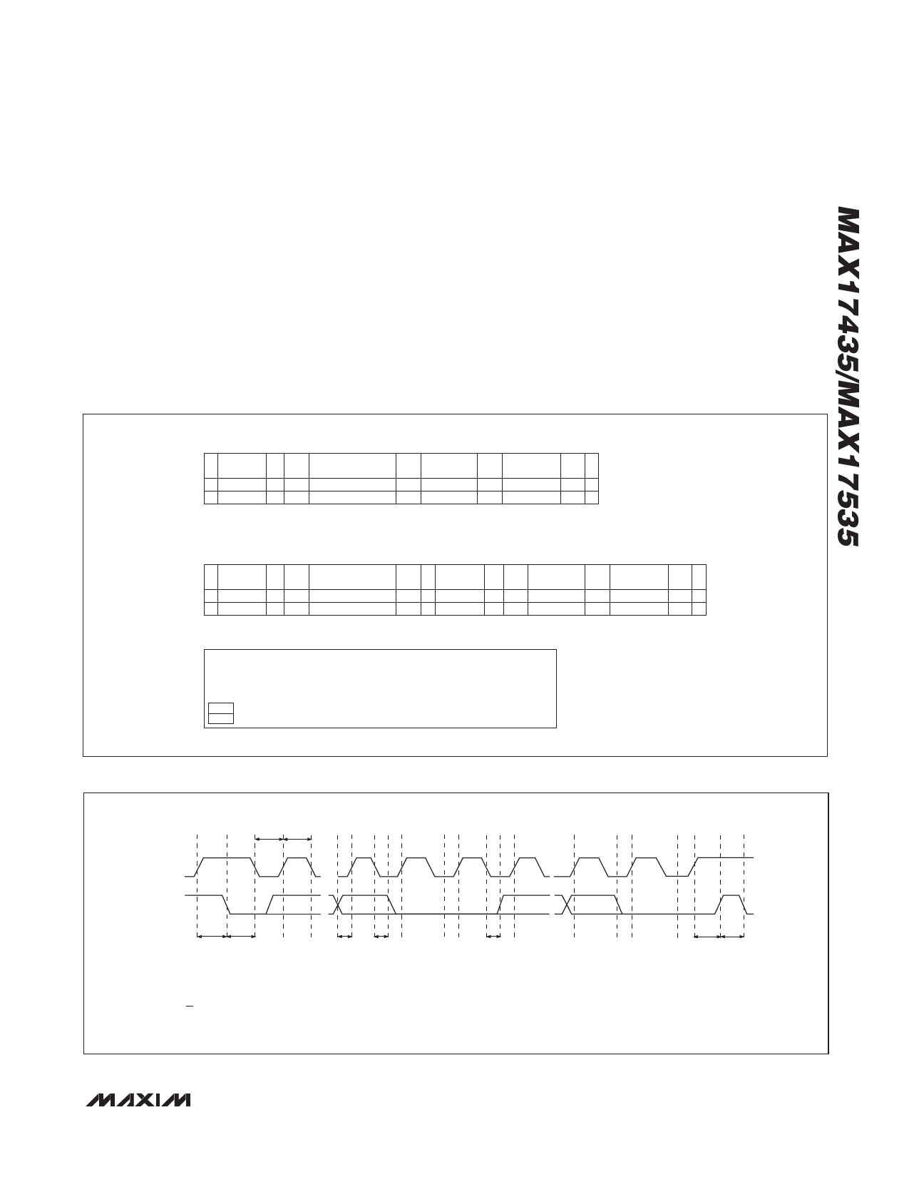
Figure 3. SMBus Write-Word and Read-Word Protocols
A
B
C
D
EF
G
tLOW tHIGH
SMBCLK
H
IJ
K
LM
SMBDATA
tSU:STA tHD:STA
A = START CONDITION
B = MSB OF ADDRESS CLOCKED INTO SLAVE
C = LSB OF ADDRESS CLOCKED INTO SLAVE
D = R/W BIT CLOCKED INTO SLAVE
E = SLAVE PULLS SMBDATA LINE LOW
tSU:DAT tHD:DAT
tHD:DAT
F = ACKNOWLEDGE BIT CLOCKED INTO MASTER
G = MSB OF DATA CLOCKED INTO SLAVE
H = LSB OF DATA CLOCKED INTO SLAVE
I = SLAVE PULLS SMBDATA LINE LOW
tSU:STO tBUF
J = ACKNOWLEDGE CLOCKED INTO MASTER
K = ACKNOWLEDGE CLOCK PULSE
L = STOP CONDITION, DATA EXECUTED BY SLAVE
M = NEW START CONDITION
Figure 4. SMBus Write Timing
______________________________________________________________________________________ 17
Share Link: 