ADN2817ACPZ-RL7(RevG) 查看數據表(PDF) - Analog Devices
零件编号
产品描述 (功能)
生产厂家
ADN2817ACPZ-RL7
(Rev.:RevG)
(Rev.:RevG)
Analog Devices

ADN2817ACPZ-RL7 Datasheet PDF : 38 Pages
| |||
Data Sheet
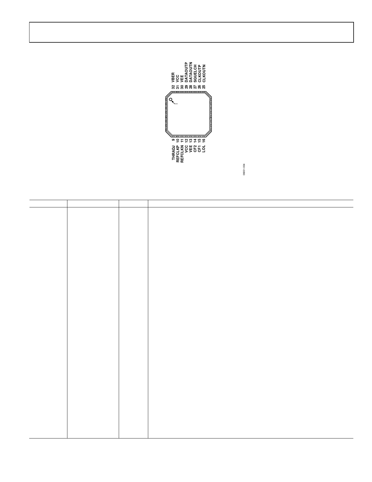
PIN CONFIGURATION AND FUNCTION DESCRIPTIONS
PIN 1
INDICATOR
BERMODE 1
VCC 2
VREF 3
NIN 4
PIN 5
SLICEP 6
SLICEN 7
VEE 8
ADN2817/
ADN2818
TOP VIEW
(Not to Scale)
24 VCC
23 VEE
22 LOS
21 SDA
20 SCK
19 SADDR5
18 VCC
17 VEE
ADN2817/ADN2818
Table 7. Pin Function Descriptions
Pin No. Mnemonic Type
1
BERMODE Digital input
2
VCC
Power
3
VREF
Analog output
4
NIN
Analog input
5
PIN
Analog input
6
SLICEP
Analog input
7
SLICEN
Analog input
8
VEE
Power
9
THRADJ
Analog input
10
REFCLKP Digital input
11
REFCLKN Digital input
12
VCC
Power
13
VEE
Power
14
CF2
Analog output
15
CF1
Analog output
16
LOL
Digital output
17
VEE
Power
18
VCC
Power
19
SADDR5
Digital input
20
SCK
Digital input
21
SDA
Digital input
22
LOS
Digital output
23
VEE
Power
24
VCC
Power
25
CLKOUTN Digital output
26
CLKOUTP Digital output
27
SQUELCH Digital input
28
DATAOUTN Digital output
29
DATAOUTP Digital output
30
VEE
Power
31
VCC
Power
32
VBER
Analog output
EPAD
Power
NOTES
1. THE EXPOSED PADDLE ON THE BOTTOM OF THE PACKAGE
MUST BE CONNECTED TO VEE.
Figure 5. Pin Configuration
Description
Set this pin to logic low to enable analog voltage output mode for BER monitor.
Power for Input Stage, LOS.
Internal VREF Voltage. Decouple to ground with a 0.1 µF capacitor.
Differential Data Input. CML.
Differential Data Input. CML.
Differential Slice Level Adjust Input.
Differential Slice Level Adjust Input.
GND for the Limiting Amplifier, LOS.
LOS Threshold Setting Resistor.
Differential REFCLK Input. 10 MHz to 200 MHz.
Differential REFCLK Input. 10 MHz to 200 MHz.
VCO Power.
VCO Ground.
Frequency Loop Capacitor.
Frequency Loop Capacitor.
Loss of Lock Indicator. Active high, LVTTL.
FLL Detector Ground.
FLL Detector Power.
Slave Address Bit 5.
I2C Clock Input.
I2C Data Input.
Loss of Signal Detect Output. Active high, LVTTL.
Output Buffer, I2C Ground.
Output Buffer, I2C Power.
Differential Recovered Clock Output. CML.
Differential Recovered Clock Output. CML.
Disable Clock and Data Outputs. Active high, LVTTL.
Differential Recovered Data Output. CML.
Differential Recovered Data Output. CML.
Phase Detector, Phase Shifter Ground.
Phase Detector, Phase Shifter Power.
This pin represents BER when analog BERMON is enabled with 3 kΩ to VEE.
Exposed Paddle. The Exposed paddle on the bottom of the package must be connected to VEE.
Rev. G | Page 11 of 38
Share Link: