AS3910-BQFP 查看數據表(PDF) - austriamicrosystems AG
零件编号
产品描述 (功能)
生产厂家
AS3910-BQFP Datasheet PDF : 47 Pages
| |||
AS3910
Data Sheet - Application Information
8.9.1 Serial Peripheral Interface (SPI)
Maximum Operation Frequency of the Serial Peripheral Interface is 20 MHz.
Table 6. Serial Peripheral Interface (4-wire Interface) Signal Lines
Name
Signal
Signal Level
SEN
Digital Input with pull down
CMOS
SDATAI
Digital Input
CMOS
SDATAO
Digital Output with tristate
CMOS
SCLK
Digital Input
CMOS
Description
SPI Enable
Serial Data input
Serial Data output
Clock for serial communication
8.9.2 SPI Operation MODE Bits
When signal SEN is low, the SPI interface is in reset and SDATAO is in tristate; when it is high, SPI interface is enabled. It is recommended to
keep signal SEN low whenever the SPI interface is not in use. SDATAI is sampled at the falling edge of SCLK. All communication is done in
blocks of 8 bits (bytes). First two bits of first byte transmitted after low to high transition of SEN define SPI operation mode. Table 7 defines
possible modes:
Table 7. SPI Operation Patterns <A7-A6>
MODE Pattern (com. bits)
MODE Related Data
MODE
MODE
Register Address
Register Data
M1 M0 C5 C4 C3 C2 C1 C0 D7 D6 D5 D4 D3 D2 D1 D0
WRITE Mode
0 0 A5 A4 A3 A2 A1 A0 WD7 WD6 WD5 WD4 WD3 WD2 WD1 WD0
READ Mode
0 1 A5 A4 A3 A2 A1 A0 RD7 RD6 RD5 RD4 RD3 RD2 RD1 RD0
FIFO Load
1 0 0 0 0 0 0 0 WD7 WD6 WD5 WD4 WD3 WD2 WD1 WD0
FIFO Read
1 0 1 1 1 1 1 1 RD7 RD6 RD5 RD4 RD3 RD2 RD1 RD0
COMMAND Mode 1 1 C5 C4 C3 C2 C1 C0
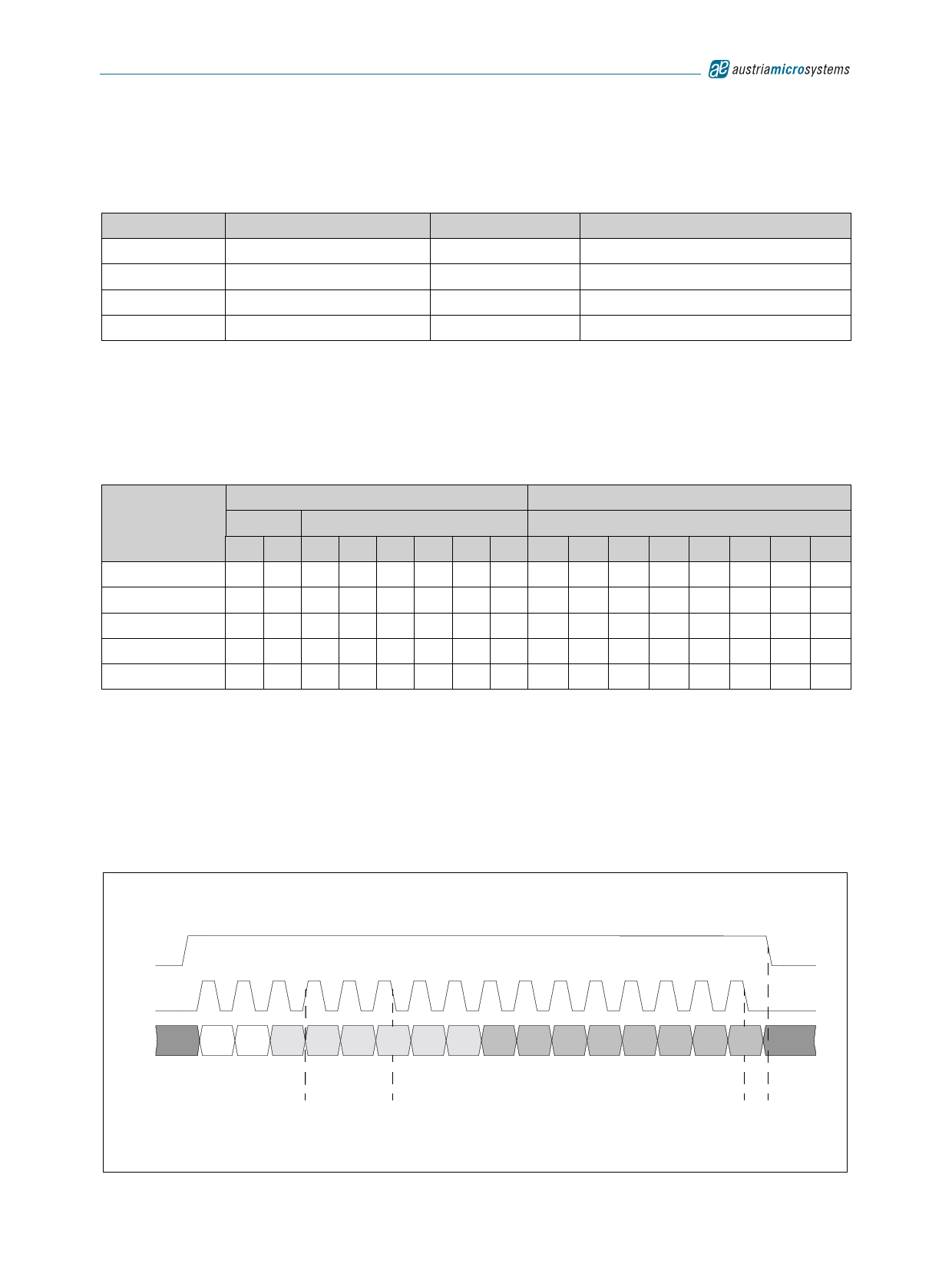
8.9.3 Writing of Data to Addressable Registers (WRITE Mode)
SDATAI is sampled at the falling edge of SCLK (see Figure 5, Figure 6). A SEN LOW pulse indicates the end of the WRITE command after
register has been written. Auto incrementing address is supported, which means that if after the address and first data byte some additional data
bytes are sent, they are then written to addresses incremented by 1. In case the command is terminated by putting SEN low before a packet of 8
bits composing one byte is sent, writing of this register is not performed. In case the register on the defined address does not exist or it is a read
only register, no write is performed. Following examples show cases of writing a single byte and writing multiple bytes with auto-incrementing
address.
Figure 5. Writing of a Single Byte (falling edge sampling)
SEN
SCLK
SDATAI
X0
0 A5 A4 A3 A2 A1 A0 D7 D6
Two leading
Zeros indicate
WRITE Mode
SCLK raising
edge data is
transferred from
µC
SCLK
falling edge
Data is sampled
D5 D4
D3 D2 D1 D0
X
Data is moved to
Address
A5-A0
SEN falling
edge signals
end of WRITE
Mode
www.austriamicrosystems.com/HF_RFID_Reader/AS3910
Revision 2.3
17 - 47
Share Link: 