AS3910-BQFP 查看數據表(PDF) - austriamicrosystems AG
零件编号
产品描述 (功能)
生产厂家
AS3910-BQFP Datasheet PDF : 47 Pages
| |||
AS3910
Data Sheet - Application Information
8.9.5 Sending Direct Commands
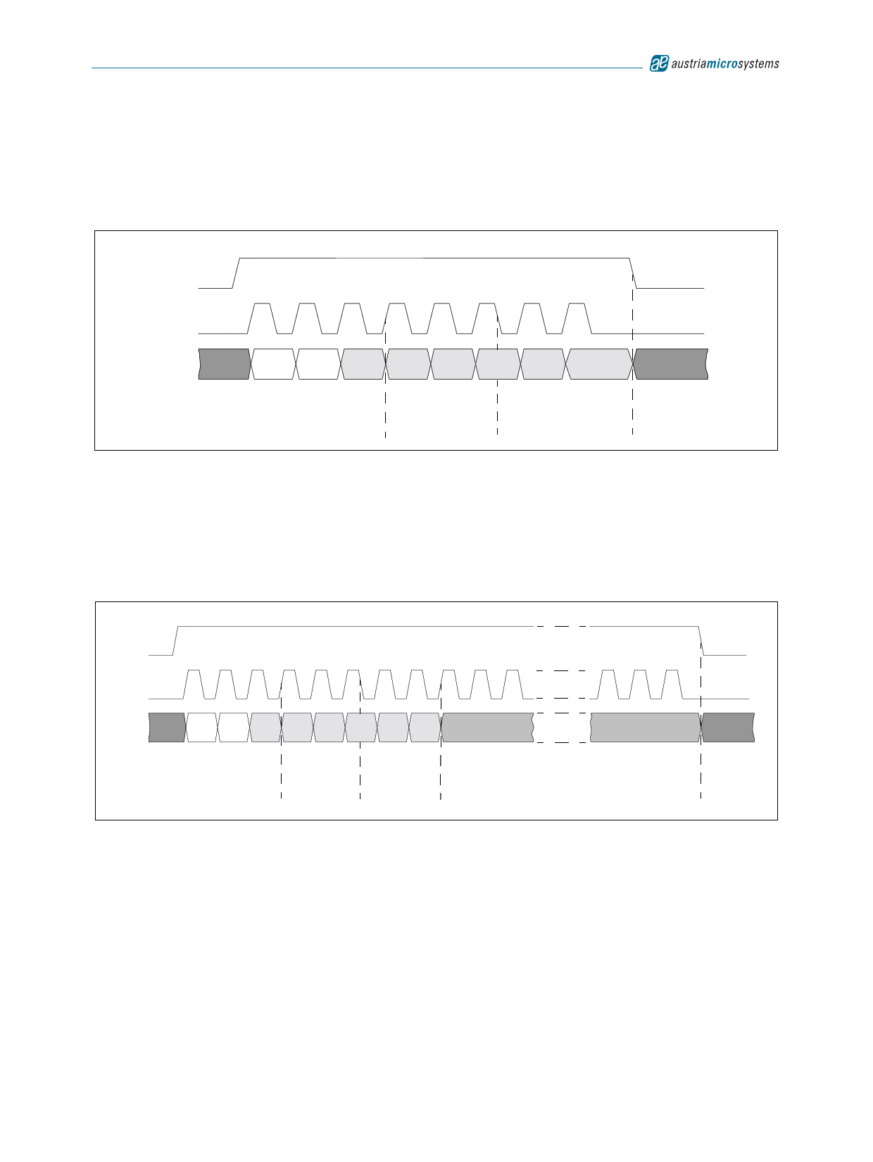
Direct commands have no arguments, so a single byte is sent. Command mode is entered if the SPI is started with two leading ONE. After the
COMMAND mode code 11 (see Table 9), the six bit command code is sent MSB to the LSB. The command is executed on falling edge of SEN.
During the direct command execution, starting another activity over the SPI interface is not allowed.
Figure 8. Sending Direct Commands
SEN
SCLK
SDATAI
X
1
1
Two leading
ONE indicate
COMMAND
Mode
C5
C4
C3
SCLK raising
edge data is
transferred from
µC
C2
C1
C0
SCLK
falling edge
Data is sampled
X
SEN falling edge
signals start of
command execution
8.9.6 Loading Transmitting Data into FIFO
Loading the transmitting data into the FIFO is similar to writing data into an addressable registers. Difference is that in case of loading more bytes
all bytes go to the FIFO. The command mode code 10 indicates FIFO operations. In case of loading transmitting data into FIFO all bits <C5 –
C0> are set to 0. Then a bit-stream, the data to be sent (1 to 32 bytes), can be transferred. In case the command is terminated by putting SEN
low before a packet of 8 bits composing one byte is sent, writing of that particular byte in FIFO is not performed. Figure 9 shows how to load the
Transmitting Data into the FIFO.
Figure 9. Loading Transmitting Data into FIFO
SEN
SCLK
SDATAI
X1
0
10 pattern
indicates
FIFO mode
00
00
0
0
SCLK raising
edge data is
transferred from
µC
SCLK
falling edge
Data is sampled
Start of
payload
Data
1 to 32
bytes
X
SEN falling
edge signals
end of
COMMAND
Mode
8.9.7 Reading Received Data from FIFO
Reading received data from the FIFO is similar to reading data from an addressable registers. Difference is that in case of reading more bytes
they all come from the FIFO. The command mode code 10 indicates FIFO operations. In case of reading the received data from the FIFO all bits
<C5 – C0> are set to 1. On the following SCLK rising edges the data from FIFO appears as in case of read data from addressable registers. In
case the command is terminated by putting SEN low before a packet of 8 bits composing one byte is read that particular byte is considered
unread and will be the first one read in next FIFO read operation.
8.9.8 Interrupt Interface
When an interrupt condition is met the source of interrupt bit is set in the Interrupt Register and the INTR pin transitions to high.
The microcontroller then reads the Interrupt Register to distinguish between different interrupt sources. After the Interrupt Register is read its
content is reset to 0 and INTR pin signal transitions to low.
Note: There may be more then one Interrupt Register bit set in case the microcontroller did not immediately read the Interrupt Register after
the INTR signal was set and another event causing interrupt occurred.
www.austriamicrosystems.com/HF_RFID_Reader/AS3910
Revision 2.3
19 - 47
Share Link: 